FDSOI is gaining traction in the market place. At their foundry forum in May, Samsung announced they have 17 FDSOI products in high volume manufacturing (you can read Tom Dilliger’s write up of the Samsung Foundry Forum here). At SEMICON West in July, GLOBALFOUNDRIES (GF) announced FDSOI design wins worth $2 billion dollars in revenue with $1 billion dollars booked in 2017 and another $1 billion dollars in revenue booked in the first half of 2018. With the emergence of FDSOI I thought it would be useful to review who the players are in the market and what their current and planned processes look like (I recently did a similar leading-edge analysis for FinFETs available here).
FDSOI Ecosystem
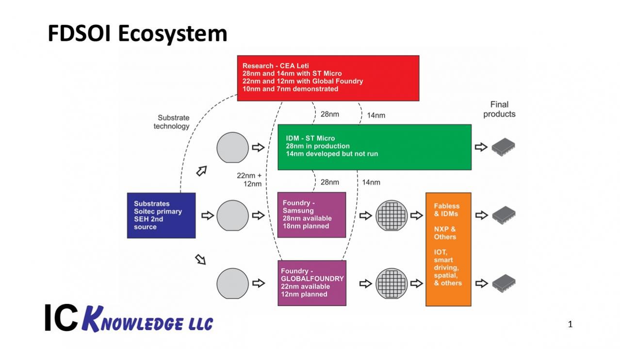
The FDSOI Ecosystem is illustrated in figure 1.
CEA Leti has served as the key research group in the development of FDSOI working with ST Micro on 28nm and 14nm processes and working with GF on 22nm and 12nm processes.
FDSOI requires engineered substrates with very thin single crystal silicon layers on buried insulator layers to insure the channel region is fully depleted. The primary supplier of FDSOI substrates is Soitec with SEH as a second source (I have written more on Soitec and their FDSOI substrates here and have another article on Soitec due to be published shortly).
The companies producing FDSOI processes are ST Micro as an IDM with 28nm in production, Samsung foundry with 28nm in production and 18nm planned, and GF foundry with 22nm in production and 12nm planned.

ST Micro
ST Micro introduced 28nm FDSOI in 2012 that is produced in their Crolles II – 300mm wafer fab. The 28nm FDSOI process offers a 32% to 84% improvement in performance over ST Micro’s 28nm bulk process. ST Micro also developed a 14nm process with CEA Leti but it is not in production. ST Micro has reportedly begun working with GF on GF’s 22FDX FDSOI process so long-term ST Micro may not continue to produce their own FDSOI and may move to a fabless model for this technology. Crolles II is a relatively low capacity 300mm fab and ST Micro makes other things in the fab, so FDSOI volumes are likely not large.
Samsung
Samsung licensed ST Micro’s 28nm FDSOI process and used it to create Samsung’s 28FDS process. 28FDS entered production in 2015 and is producing 17 high volume products as previously mentioned. An 18nm follow-on process is in development and due next year.
28FDS provides fmax >400GHz for RF applications, embedded MRAM nonvolatile memory and is automotive qualified. 28FDS has a 1.0 volt Vdd.
18FDS is planned for 2019, it features a back end taken from Samsung’s mature 14nm FinFET technology and provides a 35% area reduction from 28FDS. 18FDS also provides a 22% performance improvement and 37% power reduction from 28FDS. The Vdd for 18FDS is 0.8 volts.
Samsung has significant foundry capacity and can ramp FDSOI to very high volumes as needed.
GLOBALFOUNDRIES (GF)
GF’s 22FDX process entered production in 2017 and offers a 400GHz fmax, embedded MRAM nonvolatile memory and is automotive qualified. 22FDX can operate down to 0.4 volts for low power applications. There are four versions available offering, low power, high performance, low leakage or RF & analog. 22FDX is based on ST Micro’s 14nm process for the front end and the back end is optimized for cost with 2 double patterned layers and the balance of the layers being single patterned.
A follow-on 12FDX process was originally due in 2019 but GF is holding off introduction of the process because customers are just now designing and ramping up products on 22FDX. Development of 12FDX is proceeding well and it will be introduced when needed, we estimate this will be around 2020. 12FDX will offer 20% performance improvement over 22FDX.
GF is producing 22FDX in their Dresden fab and has significant capacity in place. A fab being brought up in China will also become a source for FDSOI capacity in the future.
Comparison
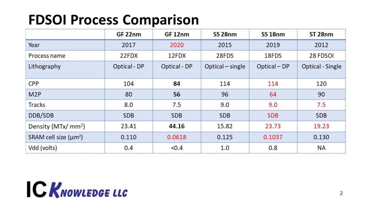
Figure 2 compares the process density metrics for GF, Samsung and ST Micro. In terms of the current FDSOI offerings, GF’s 22FDX is the clear leader in density and also offers the lowest operating voltage. Samsung’s planned 18FDS process will likely be slightly denser than GF’s current FDX22 process but GF’s planned 12FDX process will once again establish GF as the clear FDSOI density leader.

Figure 2. FDSOI process comparison
One thing I have a hard time understanding is why Samsung isn’t more aggressive on operating voltage. Power consumption is proportional to the operating voltage squared and FDSOI is targeted at many low power applications. GF has a clear lead in low power operation with their 0.4 volts Vdd.
Discussion
FDSOI is being positioned as a lower cost alternative to FinFETs for IOT, automotive and mobile applications. The specific FDSOI process choices in terms of density and number of interconnect layers position them to be less expensive than the denser FinFET processes. FinFET processes are also typically not well suited to analog and RF applications. We believe that at the same node and number of metal layers FinFET processes and FDSOI processes are similar in cost but once again the FDSOI processes are positioned differently, for example GF offers 22FDX with 8 metal layers as a lower cost alternative to their 14nm FinFET process that has 11 or more metal layers. 22FDX has a lower mask count than 14nm FinFET and has lower cost per wafer, the 14nm FinFET process is denser and better suited for large – high-performance designs but 22FDX offers lower cost, nearly as good digital performance and better analog and RF performance at lower power.
FDSOI also offers the unique capability for back biasing to set threshold voltages and tune performance and power consumption. Accessing the back gate for back biasing only requires a 1% area penalty while delivering a unique and useful capability not available in other processes.
FDSOI also offers lower design costs than FinFETs with 28FDS and 22FDX offering similar design costs to 28nm bulk whereas 14nm FinFET processes have design costs that are roughly 2x the design costs for 28nm bulk. 7nm FinFET design costs are expected to be even higher than 14nm design costs.
Conclusion
We believe that FDSOI is well positioned to capture market share in IOT, 5G, and automotive applications. FinFETs will continue to be the technology of choice for applications with a lot of digital logic and that require the highest possible performance. After many years of development FDSOI is poised to become a main stream alternative.


Musk’s Orbital Compute Vision: TERAFAB and the End of the Terrestrial Data Center