




The bottlenecks are becoming interconnected
Artificial intelligence is changing what the semiconductor industry must deliver. As AI models grow and applications expand, the challenge is no longer simply to make individual chips faster or more efficient. It is to build complete computing systems that can deliver greater performance, move more data and consume less energy, all while bringing new technologies to market faster.
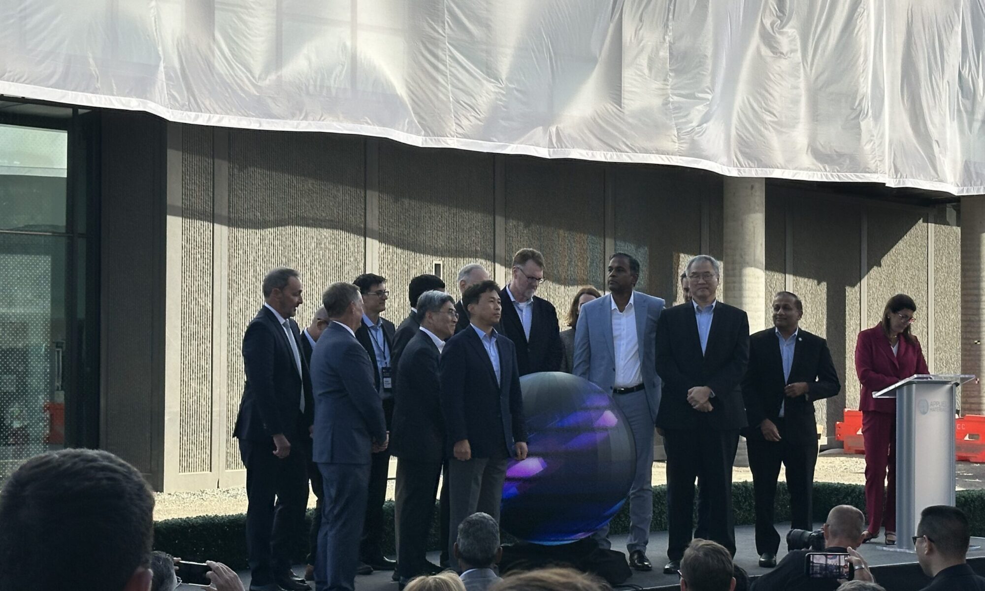
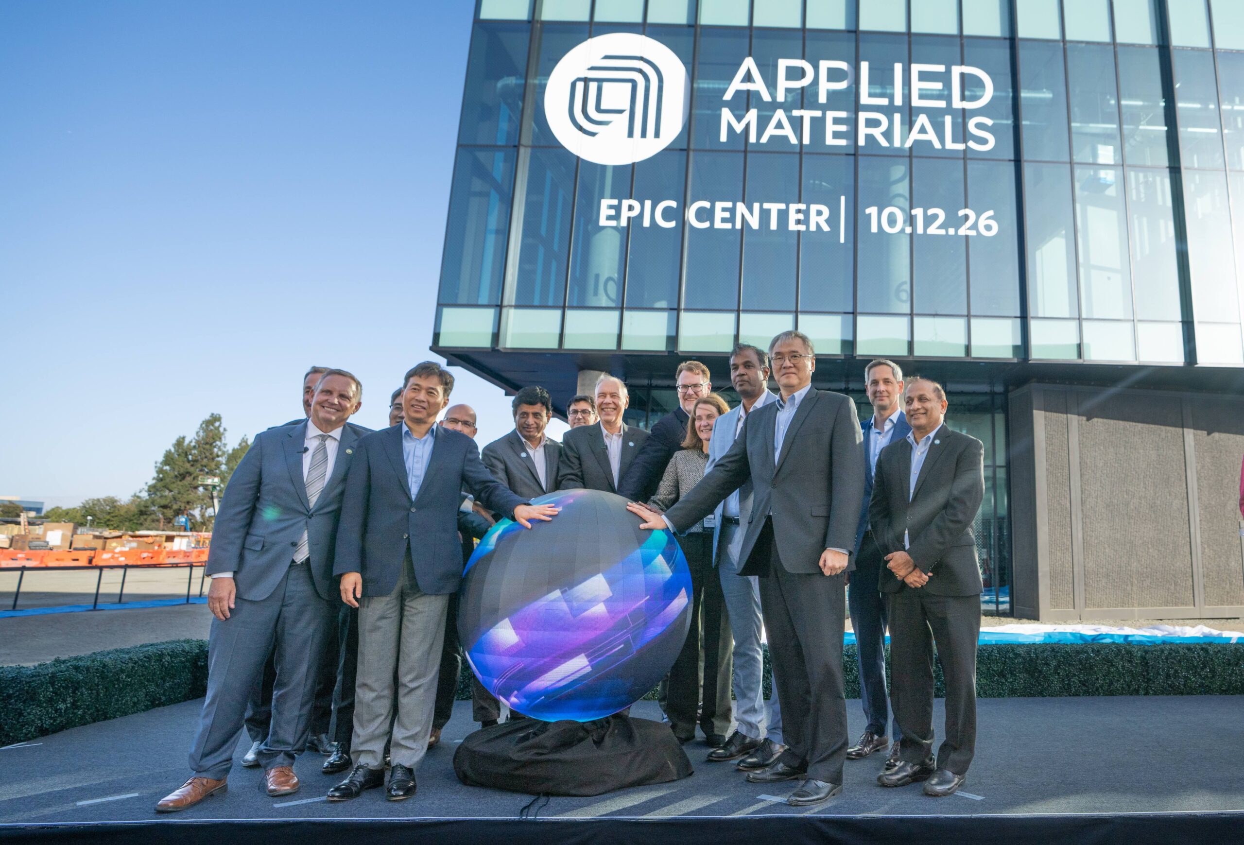
That was a central theme of the unveiling of Applied Materials’ EPIC Center, where leaders from across the semiconductor ecosystem discussed the technical demands of the AI era and the need to rethink how innovation happens.
The event brought together perspectives from SK hynix, TSMC, Micron, Intel, Samsung, Broadcom, NVIDIA and Qualcomm, alongside Applied Materials. Although these companies occupy different positions in the semiconductor value chain, their contributions pointed to a common challenge: advances in one part of the system increasingly depend on progress in others.
AI computing places intense demands on processors, memory, interconnects, advanced packaging and power efficiency. Improving one component in isolation cannot necessarily overcome a bottleneck elsewhere in the system.
Memory is a particularly important example. As AI workloads grow, moving data between memory and compute becomes a major constraint on both performance and energy consumption. High-bandwidth memory (HBM), closer integration of memory and logic, and new approaches to packaging are therefore becoming central to system design—not simply considerations to address after a processor has been developed.
Interconnects create another challenge. Large AI systems distribute workloads across multiple processors, making communication speed, latency and energy use increasingly consequential. Approaches such as advanced chip integration and co-packaged optics could help address these constraints, but they require progress in materials, processes, packaging and system architecture to work together.
Thermal management adds another layer of complexity. As more compute and memory are brought together, the industry must find ways to manage heat while maintaining performance and efficiency. These are not isolated engineering problems. They are connected challenges that span the technology stack.
Why no company can solve the problem alone
The perspectives shared at the EPIC Center event highlighted how closely linked these challenges have become. Memory suppliers must consider the needs of compute architectures. Chip and system designers need to account for the capabilities and limitations of manufacturing processes, packaging and materials. Equipment and materials innovators must understand how their technologies affect the performance of the final system.
That interdependence changes the economics and timing of innovation. If companies work independently and only integrate their technologies late in development, problems may emerge after substantial time and resources have already been invested. Resolving those problems can mean additional development cycles and delayed products.
Earlier collaboration can expose constraints sooner, enable teams to evaluate trade-offs together and help align development priorities around system-level outcomes. The objective is not to eliminate competition. It is to recognize where shared technical challenges require coordinated innovation.
EPIC represents a response to a system-level challenge
Applied Materials’ EPIC Center is designed to support this kind of collaboration, bringing industry partners together to work on materials, processes and equipment relevant to future semiconductor technologies. Its significance lies not simply in the research infrastructure, but in the opportunity to connect expertise across the ecosystem and address difficult integration challenges earlier.
The wider message from the event was that AI’s growing demands will require more than continued advances in individual devices. The industry must increasingly innovate across the full technology stack, with performance, power, integration and manufacturability considered together.
That is the industry challenge: AI is making collaboration across company and technology boundaries a practical requirement for continued semiconductor progress.
But recognizing the need to collaborate is only the first step. How can companies establish that collaboration in practice? The companion article, “From Sequential R&D to Trusted Co-Innovation: The EPIC Model for Semiconductor Innovation”, explores the operating model behind faster, earlier and more trusted collaboration.
Read the press release about the October 12th unveiling of the EPIC Center.
Also Read:
TSMC’s AI Expansion Signals a Broader Shift in Computing
Terafab’s Single Roof: Why Packaging, Not Lithography, Decides High Volume
Why Semiconductor AI Starts with Data, Not Algorithms
Share this post via:


Rethinking Phase Jitter: An Algorithmic Approach to Signal Integrity