







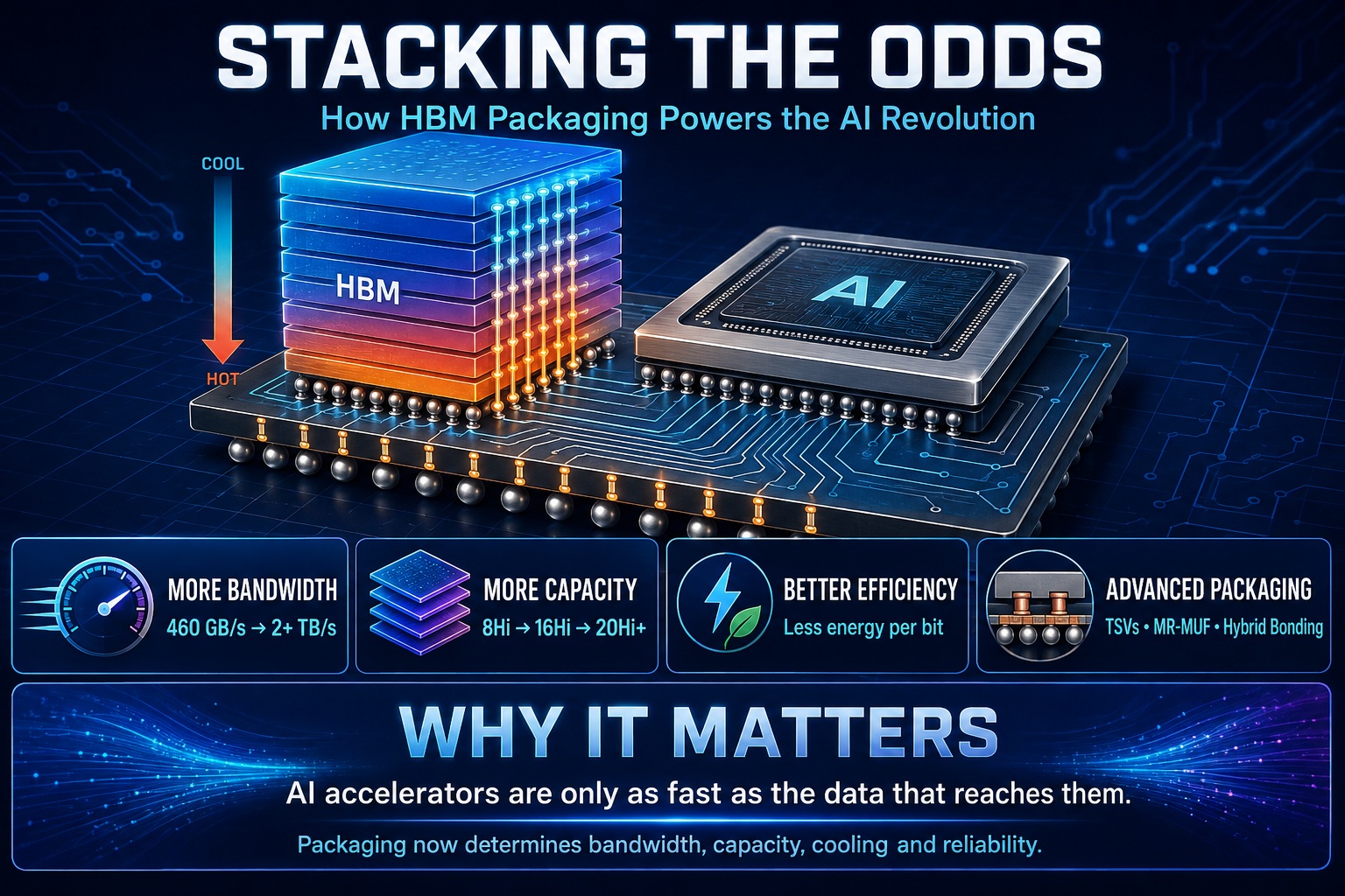
SK hynix’s Hot Chips 2026 presentation explains how High Bandwidth Memory (HBM) is evolving to meet the extraordinary memory requirements of artificial intelligence. Its central message is that future progress will depend not only on better DRAM circuits but also on advanced packaging, denser vertical integration, improved thermal management, and closer coordination between memory and processor design.
HBM stacks multiple DRAM dies vertically above a base die, connecting them with through-silicon vias, or TSVs. The complete memory package sits beside a GPU or accelerator on a silicon interposer and communicates through thousands of parallel connections. Compared with conventional memory, this wide interface provides exceptional bandwidth while occupying less board space. The presentation compares four HBM3E packages with twelve GDDR6 devices: the HBM configuration offers 144 gigabytes of capacity and roughly four terabytes per second of bandwidth while using about half the area. HBM3E is also shown as consuming substantially less energy per transferred bit.
AI creates three simultaneous requirements: higher bandwidth for parallel computation, greater capacity for large models and datasets, and better power efficiency for data-center cooling and operating costs. Each HBM generation attempts to advance all three. According to the presentation, maximum bandwidth rises from approximately 460 gigabytes per second for HBM2E to 717 gigabytes per second for HBM3, 1,024 gigabytes per second for HBM3E, and 2,048 gigabytes per second for HBM4. HBM4 doubles the total interface width from 1,024 to 2,048 data connections.
These gains make manufacturing dramatically harder. HBM4 contains more than 20,000 TSVs and approximately 16,148 micro-bumps. Its larger package and higher stack create difficult problems involving wafer thinning, die warpage, bump uniformity, narrow-gap filling, joint reliability, and heat removal. A defect in one layer can affect the value of the completed stack, so precise inspection and “known-good stacked die” testing become essential.
SK hynix highlights mass reflow with molded underfill, or MR-MUF, as a key production technology. Unlike thermo-compression bonding, which attaches dies individually with heat and force, mass reflow bonds multiple connections together and then fills the stack with protective material. This approach offers greater productivity and lower thermal resistance, although it becomes increasingly sensitive to warpage and narrow gaps. Advanced MR-MUF enabled SK hynix to develop a 16-layer HBM3E stack containing 48 gigabytes while remaining within a package height of 775 micrometers.
For stacks of 20 dies or more, the presentation identifies hybrid bonding as a promising successor. Hybrid bonding joins dielectric surfaces and copper connections directly, eliminating conventional solder micro-bumps. The resulting connections can be much narrower, permitting more TSVs and higher bandwidth. Removing bumps also creates room for thicker, mechanically stronger DRAM dies within the same height limit. Direct copper connections conduct heat more effectively, which becomes increasingly valuable as the number of active layers rises.
Thermal management is equally important. Greater bandwidth raises power consumption, while taller stacks make it harder for heat to escape. SK hynix’s proposed i-HBM architecture inserts an electrically insulating but thermally conductive component into the hot die-to-die interface region, forming a dedicated heat path. The presentation reports a potential reduction in thermal resistance exceeding 30 percent. Advanced logic processes for the base die can further lower power, while distributing power TSVs throughout the package improves the power-delivery network.
Why does this matter? AI performance is increasingly constrained by how quickly and efficiently data can reach processors. A powerful accelerator that waits for memory wastes silicon, electricity, and cooling capacity. HBM reduces that bottleneck, but its success now depends on packaging technologies once treated as secondary manufacturing details.
Bottom line: The presentation therefore describes a larger industry transition. Memory was traditionally installed near the end of system assembly. In advanced AI packages, HBM is integrated early alongside expensive processors and interposers. It must survive stresses created by technologies such as TSMC CoWoS, redistribution-layer interposers, and embedded bridges. Consequently, memory suppliers, foundries, processor designers, and packaging companies must collaborate from the beginning. Advanced packaging is no longer merely how HBM is assembled; it is what determines whether future AI systems can achieve the required bandwidth, capacity, reliability, and energy efficiency.
Source: Jaesik Lee, SK hynix America, HC2026 presentation.
Also Read:
GenAlpha Brings a Practical Approach for Analog AI to DAC 2026
Crescent Island: Turning Memory Capacity into Agentic AI Throughput
Share this post via:



The silent killer of analog reliability: Why SPICE misses floating net