At a webinar today I listened and learned about how a tool called L-Edit can be used to layout MEMS designs plus automate the task to be more productive. I can see how the history of IC layout editing is now being repeated with MEMS because in the earliest IC layout tools we could only do manual entry of polygons, then gradually we got cells… Read More
 The RISC-V and Open-Source Functional Verification ChallengeMost of the RISC-V action at the end…Read More
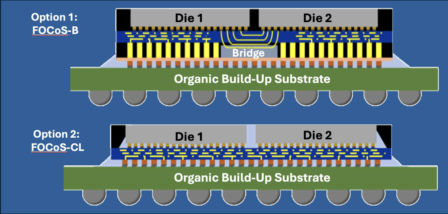 Sarcina Democratizes 2.5D Package Design with Bump Pitch Transformers2.5D package design is rapidly finding its stride…Read More
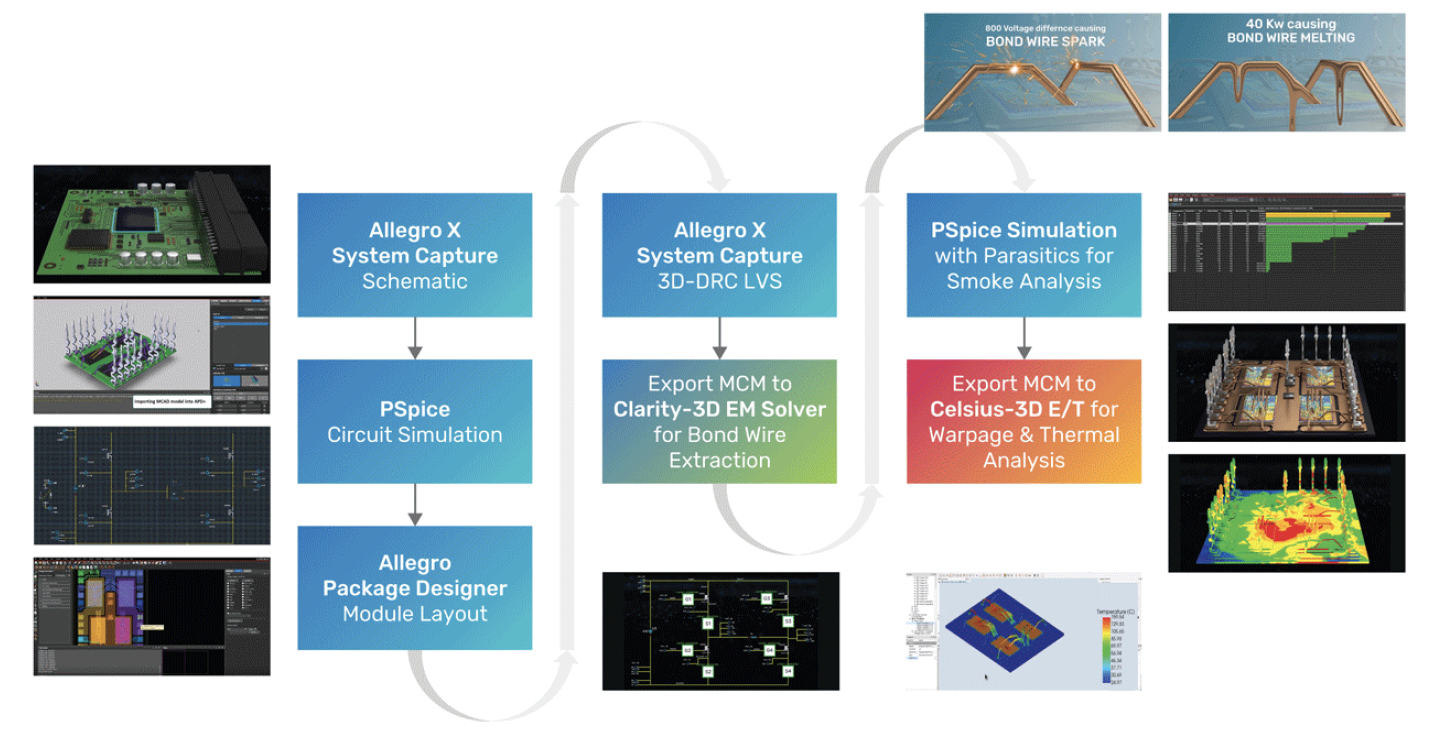 Addressing Reliability and Safety of Power Modules for Electric VehiclesAs electric vehicles (EVs) gain widespread adoption, safety,…Read More
 Shaping Tomorrow’s Semiconductor Technology IEDM 2024Anyone who has read my articles about IEDM…Read More
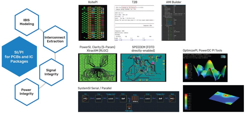 SI and PI Update from Cadence on Sigrity XSignal Integrity (SI) and Power Integrity (PI) issues…Read More
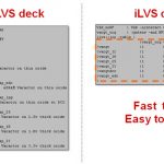
iLVS: Improving LVS Usability at Advanced Nodes
LVS Challenges at Advanced Nodes
Accurate, comprehensive device recognition, connectivity extraction, netlist generation and, ultimately, circuit comparison becomes more complex with each new process generation. As the number of layers and layer derivations increases the complexity of devices, especially Layout Dependent… Read More
IP-SoC 2011 Trip Report: IP again, new ASSP model, security, cache coherence and more
For the 20[SUP]th[/SUP] anniversary of IP-SoC, we had about ten presentations, most being really interesting; the conference has provided globally a very good level of information, speakers coming from various places like China, Belarus, The University of Aizu (Japan), University of Sao Paulo (Brazil), Silesian and Warsaw… Read More
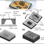
Learning About MEMS
My automobile has an air bag system that uses a MEMS (Micro Electro Mechanical System) sensor to tell it when to deploy, and I’ve read headlines talking about MEMS over the years so I decided it was about time to learn more by attending a Webinar on Wednesday, December 14th at 8AM Pacific Time.
The EDA company hosting the Webinar… Read More
View from the top: Ajoy Bose
I sat down yesterday with Dr. Ajoy Bose, CEO of Atrenta, to get his view of the future of EDA – looking through a high-power “spyglass” of sorts. I first met Ajoy when he was at Software & Technologies. I was then the VP of Engineering for Compass Design Automation and we were considering off-shoring some development. We eventually… Read More
Intel Proves Last Year’s Conventional Wisdom Wrong
Back in the 1990’s, Richard Branson, the legendary Entrepreneur and investor was asked how to become a millionaire, and he allegedly responded, “There’s really nothing to it. Start as a billionaire and then buy an airline.” I think the same principle can be applied to a large part of the Semiconductor… Read More
Synopsys Eats Magma: What Really Happened with Winners and Losers!
Conspiracy theories abound! The inside story of the Synopsys (SNPS) acquisition of Magma (LAVA) brings us back to the 1990’s tech boom with shady investment bankers and pump/dump schemes. After scanning my memory banks and digging around Silicon Valley for skeletons with a backhoe here is what I found out:
The Commission… Read More
Atrenta’s users. Survey says….
Atrenta did an online survey of their users. Of course Atrenta’s users are not necessarily completely representative of the whole marketplace so it is unclear how the results would generalize for the bigger picture, your mileage may vary. About half the people were design engineers, a quarter CAD engineers and the rest … Read More
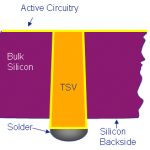
Challenges in 3D-IC and 2½D Design
3D IC design and what has come to be known as 2½D IC design, with active die on a silicon interposer, require new approaches to verification since the through silicon vias (TSVs) and the fact that several different semiconductor processes may be involved create a new set of design challenges
The power delivery network is a challenge… Read More
Low power techniques
There was recently a forum discussion about the best low power techniques. Not surprisingly we didn’t come up with a new technique nobody had ever thought of but it was an interesting discussion.
First there are the techniques that by now have become standard. If anyone wants more details on these then two good resources are… Read More





AI Semiconductor Market