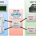
You are currently viewing SemiWiki as a guest which gives you limited access to the site. To view blog comments and experience other SemiWiki features you must be a registered member. Registration is fast, simple, and absolutely free so please,
join our community today!
Coming up on April 10th is the SEMI Silicon Valley Breakfast Forum Internet of Things—Driving the Microelectronics Revolution. It runs from 7am to 10.45am and will be held at SEMI Headquarters which is at 3081 Zanker Road in San Jose.
Widespread adoption of the Internet of Things will take time, but the movement is advancing thanks… Read More
MEMS design and fabrication is highly complex in the sense that the fabrication process heavily depends on the design, unlike IC fabrication which has a standard set of processes. A slight change in MEMS design can alter its fabrication steps to a large extent. For example, setting device parameters such as capacitance or linear… Read More
There is clearly a lot of hype about the Internet of Things (IoT) right now, but also it is clear that it will be a real market. In fact, it already is with various medical, fitness and home-appliance products already available. At CES in January, wearables was probably the biggest trend. That doesn’t always pan out (3D TV was… Read More
The most successful EDA companies typically choose a domain where they have deep knowledge, then serve a few leading-edge customers that are willing to work with a start-up in exchange for early access to that new technology. The theory is that if you can satisfy the leading-edge customer then you can also satisfy the rest of the … Read More
Handel Jones has a new white-paper out titled Why Migration to FD-SOI is a Better Approach Than Bulk CMOS and FinFETs at 20nm and 14/16nm for Price-Sensitive Markets. Handel has done an in-depth analysis of the wafer and die costs of the various approaches, bulk planar (what we have been doing up to now), FD-SOI and FinFET. The analysis… Read More
As several other recent threads on SemiWiki have pointed out, the term “wearables” is a bit amorphous right now. The most recognizable wearable endeavors so far are the smartwatch and fitness band, but these are far from the only categories of interest.
There is another area of wearable wonder beginning to get attention: clothing,… Read More
Triple Patterningby Paul McLellan on 03-19-2014 at 1:00 pmCategories: EDA, Foundries
As you can’t have failed to notice by now, 28nm is the last process node that does not require double patterning. At 20nm and below, at least some layers require double patterning. The tightest spacing is typically not the transistors but the local interconnect and, sometimes, metal 1.
In the litho world they call double patterning… Read More
I am convinced after studying out the matter, that Aldec is one of the leaders in DO254 certification. As you listen and read the news as I do about flight MA-370, you keep theorizing and wondering. This is a good time to introduce the reader to the seriousness of flight worthy electronics and the arduous process to achieve certification.… Read More
The DSP48E2 (I do not come up with these names… Could have named it a multiplier thingy) in the Xilinx 20nm UltraScale family (I do not come up with these names… Could of named it Virtex-8, or Luke-8) is simply amazing. Today was good, as I began playing with UltraScale tools and seeing how the DSP checks out. I also encourage you to check… Read More
For those of you who missed the IEEE International Solid-State Circuits Conference last month some of the presentations are now hitting the company websites. The theme of this year’s conference was SILICON SYSTEMS BRIDGING THE CLOUD:… Read More
Facing the Quantum Nature of EUV Lithography