The recent Chiplet Summit in Santa Clara was buzzing with new designs and new design methods. It felt like the industry had turned a corner at this year’s event with lots of new technology and design success on display. Siemens EDA had a large presence at the show and took home the Best in Show Award for Packaging Design. There were a … Read More
 When a Platform Provider Becomes a Competitor: Why Arm’s Silicon Strategy Changes the IncentivesMarc Evans, Director of Business Development & Marketing,…Read More
 yieldHUB Expands Its Impact with New Technology and a New WebsiteyieldHUB is a unique company that focuses on…Read More
 Architecting Intelligence: The Rise of RISC-V CPUs in Agentic AI InfrastructureSiFive’s newly announced $400 million Series G financing…Read More
 Intel, Musk, and the Tweet That Launched a 1000 Ships on a Becalmed SeaIntel, Musk, and the Tweet That Launched a…Read More
Siemens Fuse EDA AI Agent Releases to Orchestrate Agentic Semiconductor and PCB Design
Though terminology sometimes get fuzzy, consensus holds that an agent manages a bounded task with control through a natural language interface. An agentic orchestrator, itself an agent, manages a more complex objective requiring reasoning through multi-step actions and is responsible for orchestrating those actions. By… Read More
Accelerating Computational Lithography Using Massively Parallel GPU Rasterizer
As semiconductor manufacturing pushes deeper into the nanometer regime, computational lithography has evolved from a supporting step into a central pillar of advanced chip design. Mask synthesis, lithography simulation, and optical proximity correction (OPC) now demand unprecedented levels of accuracy and computational… Read More
Verification Analytics: The New Paradigm with Cogita-PRO at DVCON 2026
Cogita-PRO, developed by Vtool, introduces a transformative approach to design verification by treating it as a big data challenge rather than a traditional debugging exercise. Released in February 2026, this tool shifts the focus from manual log and waveform inspection to advanced verification analytics powered by data … Read More
Breker Hosts an Energetic Panel on Spec-Driven Verification
I was fortunate to be asked to moderate an evening panel adjacent to the first day of DVCon 2026, on AI-Driven SoC Verification starting from specs. You know my skepticism on panels, finding they rarely generate insights or controversy. This panel was quite different. Panelists were Shelley Henry (CEO, Moores Lab AI), Adnan Hamid… Read More
Formal Verification Best Practices
How do I know when my hardware design is correct and meets all of the specifications? For many years the answer was simple, simulate as much as you can in the time allowed in the schedule and then hope for the best when silicon arrives for testing. There is a complementary method for ensuring that hardware design meets the specifications… Read More
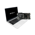
The First Real RISC-V AI Laptop
At a workshop in Boston on February 27, something subtle but important happened. Developers sat down in front of a RISC-V laptop, installed Fedora, and ran a local large language model. No simulation. No dev board tethered to a monitor. A laptop.
For more than a decade, RISC-V advocates have promised that the open instruction set… Read More
AI-Driven Automation in Semiconductor Design: The Fuse EDA AI Agent
The semiconductor industry is experiencing unprecedented growth in complexity as advanced process nodes, heterogeneous integration, and AI-driven workloads demand increasingly sophisticated chip designs. At the same time, semiconductor companies face rising design costs, increasing engineering workloads, and a shrinking… Read More
TSMC Technology Symposium 2026: Advancing the Future of Semiconductor Innovation
One of my favorite times of the year is coming (sailing season) and my favorite event of the year is coming as the company I most respect will host the best international semiconductor networking event starting here in Silicon Valley.
The 32nd annual TSMC Technology Symposium represents one of the most influential events in the … Read More
Synopsys Explores AI/ML Impact on Mask Synthesis at SPIE 2026
The SPIE Advanced Lithography + Patterning Symposium recently concluded. This is a popular event where leading researchers gather. Challenges such as optical and EUV lithography, patterning technologies, metrology, and process integration for semiconductor manufacturing and adjacent applications are all covered. This… Read More


Intel, Musk, and the Tweet That Launched a 1000 Ships on a Becalmed Sea