

The semiconductor industry is entering a new phase of complexity. Advanced nodes, heterogeneous integration, and AI-driven design workflows are placing unprecedented demands on engineering teams. While much of the focus remains on tools and methodologies, an equally critical constraint is emerging beneath the surface: infrastructure.
Every IC design company today must make a foundational decision:
How to design, build, and operate the increasingly AI-driven ECAD IT infrastructure required to deliver chips efficiently. Historically, the answer has been to build and manage it internally. But that model is becoming increasingly difficult to sustain.
The Growing Infrastructure Burden
Modern semiconductor workflows depend on a combination of:
- Distributed compute environments
- Multiple EDA toolchains from different vendors
- GPU-intensive AI/ML workloads
- Strict data security and compliance requirements
Yet the infrastructure supporting these workflows is often fragmented. Teams must stitch together cloud resources, on-prem systems, license servers, and workflow orchestration tools without compromising on uptime and performance.
Cloud providers offer scalable compute, storage, and networking. And EDA vendors provide powerful design tools. But a unified, production-ready vendor agnostic environment is hard to come by for semiconductor engineering. This results in a gap that engineering teams must fill themselves.
The Limits of the Build-It-Yourself Model
To bridge this gap, companies invest heavily in:
- CAD engineering teams
- DevOps and cloud specialists
- Custom scripts and automation frameworks
While this approach provides flexibility, it introduces significant overhead. Infrastructure must be continuously maintained, updated, and debugged. Misconfigurations, workflow failures, and resource inefficiencies are common.
More importantly, this effort does not directly contribute to product differentiation. Engineering teams end up spending time maintaining infrastructure rather than advancing design. As AI-driven workflows accelerate the increase in design complexity, the above burden grows even more.
A Shift Toward Engineering Infrastructure Platforms
An alternative approach is beginning to gain traction: the engineering infrastructure platform.
Rather than assembling infrastructure components manually, teams can deploy a platform that provides:
- Pre-integrated environments
- Vendor-neutral tool support
- Automated orchestration
- Built-in observability and security
This model abstracts the complexity of infrastructure while preserving flexibility. Tuple Technologies’ Stratos platform is one example of this approach, designed specifically for semiconductor workflows.
Below is a quote from Vamshi Kothur, CEO of Tuple Technologies.
“The Stratos Platform was built to solve the most critical bottleneck in semiconductor innovation: the infrastructure gap. By enabling rapid environment provisioning in minutes rather than weeks and offering a truly vendor-neutral architecture, we empower design teams to scale AI and HPC workloads seamlessly across any self-hosted, cloud or hybrid environment. Our mission at Tuple Tech is to provide a continuous, AI-driven automation layer that eliminates vendor lock-in and manual remediation, allowing engineers to focus on what matters most—accelerating the path to tapeout.”
What Changes with a Platform Approach
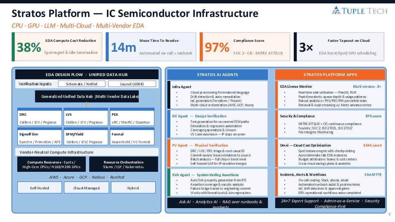
Stratos is built on Infrastructure-as-Code (IaC) principles and enables teams to deploy and operate environments across on-premises, hybrid, and cloud configurations.
Key capabilities include:
- Rapid environment provisioning — in minutes rather than weeks
- Support for multiple EDA vendors without lock-in
- Integration of AI and HPC workloads into existing flows
- Continuous monitoring, alerting, and automated remediation
The impact changes how teams work. Engineers shift from managing infrastructure to focusing on design execution.
CAD teams no longer need to manually manage licenses, debug workflows, or coordinate across fragmented environments. Instead, they operate within a unified platform where infrastructure is automated and observable.
Quantifiable Impact
The benefits of this approach are measurable: (as reported by Tuple Technologies)
- Up to 70% reduction in infrastructure development time
- Provisioning in minutes instead of weeks
- Average 38% reduction in GPU and compute costs through multi-cloud optimization
- 43% reduction in cloud computing costs in Pegasus sign-off workloads (customer case study)
In addition:
- License utilization improves through real-time analytics
- Downtime is minimized through proactive incident management
- Disaster recovery is accelerated using IaC-based reconstruction
These improvements directly translate into faster design cycles and lower operational costs.
Key Differentiators
Several characteristics distinguish an engineering infrastructure platform from traditional approaches:
Vendor Neutrality: Teams can combine tools from multiple vendors without workflow fragmentation.
Multi-Cloud Optimization: Workloads are dynamically executed where compute resources are most efficient.
Operational Intelligence: Failures are detected and resolved automatically through integrated monitoring and escalation.
Built-In Security: Continuous compliance and threat detection are embedded into the platform.
Domain-Specific Support: Real-time support from engineers familiar with semiconductor workflows ensures rapid resolution of issues.
Why This Matters Now
As semiconductor design becomes increasingly data- and compute-intensive, infrastructure is no longer a secondary concern. It is a critical enabler of engineering productivity.
Companies that continue to rely on fragmented, manually managed environments risk:
- Slower time-to-market
- Higher compute and operational costs
- Reduced engineering efficiency
By contrast, those adopting a platform approach gain:
- Faster iteration cycles
- Greater flexibility across tools and environments
- Improved reliability and scalability
Summary
The semiconductor industry has long focused on advancing tools and methodologies. The next frontier is infrastructure. Moving from fragmented systems to unified engineering platforms represents a fundamental shift. A unified engineering platform can significantly impact productivity, cost, and competitiveness.
Learn more at https://www.tupletechnologies.net/
Also Read:
Tuple Technologies at the 2025 Design Automation Conference #62DAC
CEO Interview with Geoffrey Rodgers of Chameleon Semiconductor
Bronco AI Webinar: Full-Chip SoC Debug in 15 Minutes
Share this post via:


Comments
There are no comments yet.
You must register or log in to view/post comments.