Corporate layoffs are always a touchy subject. I think that’s because there is skepticism that one round of layoffs can turn into two, then if business still doesn’t improve the spiral accelerates into more rounds. Too many rounds indicate management didn’t really have a clue what was going on in the business, instead trying to … Read More
 Agentrys Designs a Real Chip with its Multi-Agent WorkforceThe face of EDA is changing. For forty…Read More
 Must-See DAC Panel – Build vs Buy: Who Owns the Intelligence Behind Tomorrow's Chips?This year, DAC will be buzzing about AI…Read More
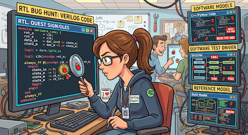 The Other Side of Bug LocalizationAutomated debugging – starting from an unexpected behavior…Read More
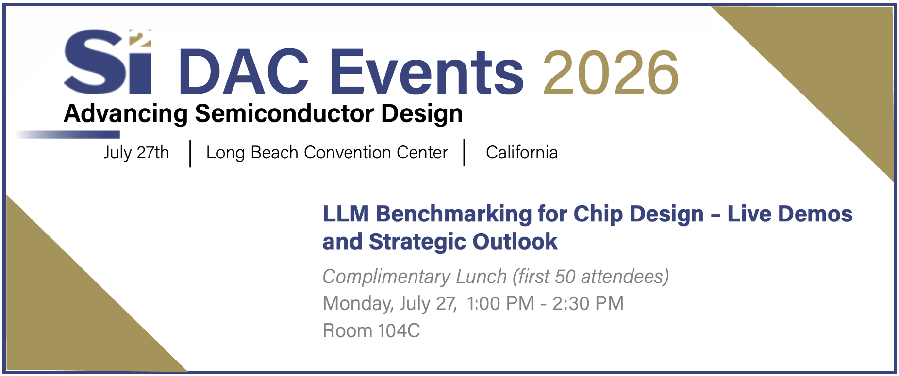 Agentrys Weighs in on LLM Benchmarking for Chip Design at DAC 2026Si2 is conducting quite a few sessions at…Read More
Reducing Data Centre Cooling by 40%
Living in Oregon has many benefits, including access to cheap electricity thanks to the plentiful river systems that provide hydro power and a growing green power business fueled by wind and sun. Many of the world’s largest data centers are located in Oregon for access to this cheap electricity, and Google has a sizable investment… Read More
IMEC Technology Forum at SEMICON – Coventor could save you billions!

The development of leading edge semiconductor technology is incredibly expensive, with estimates ranging from a few to several billion dollars for new nodes. The time to develop a leading edge process is also a critical competitive issue with some of the largest opportunities awarded based on who is first to yield on a new node.… Read More
IoT Tutorial: Chapter 8 – Introducing Internet-of-Things (BigData) Steams and Analytics
Introduction to IoT Analytics – IoT Analytics vs. BigData Analyticss. In the previous chapter of the IoT tutorial, we explained the affiliation between IoT data and BigData, given that IoT data expose the Vs of BigData. We also illustrated the activities comprising IoT data processing applications, such as data selection, validation,… Read More
IMEC-Horizontal Nanowires for 5nm at the VLSI Technology Symposium
At the VLSI Technology Symposium, IMEC presented a paper entitled “Gate-All-Around MOSFETs based on Vertically Stacked Horizontal Si Nanowires in a Replacement Metal Gate Process on Bulk Silicon Wafers”. I have wanted to blog about this paper since the symposium was held but also wanted to tie it in with an interview… Read More
10nm Will Be an Epic Process Node!

In the history of the fabless semiconductor industry the foundries have always been a process node or two behind the leading semiconductor manufacturers. Starting in Q1 2017, for the first time in fabless semiconductor history, the foundries will have a process node advantage. This is horrible news for some but great news for … Read More
Can one process handle IIoT safety and security?
SemiWiki had another article recently making the case that in IoT applications, safety and security are intertwined, adding that both are important, but they are not the same thing. Mentor Graphics has weighed in with a new white paper trying to tie both issues to a methodology.
Industrial IoT – or IIoT as you’ll often see in shorthand… Read More
Samsung Embraces Both Public And Private Cloud With Joyent Acquisition
As the mobile industry growth slows and looks to growth in IoT, companies like Samsung Electronics are looking for ways to initiate change or adapt to the new climate around them. One of the ways mobile companies are going to be profitable in the future is through offering, building and sometimes hosting those services beyond just… Read More
Big Data Lessons from the LHC
Big Data techniques have become important in many domains, not just to drive marketing strategies but also for semiconductor design, as evidenced by Ansys’ recent announcements around their use of Big Data analytics. And they should become even more important in the brave new world of the IoT. So it makes sense to look at an organization… Read More
Not-so-ulterior motive leads SoftBank to ARM
This week’s £24.3B offer for ARM Holdings plc from SoftBank has been widely viewed as Brexit reflexit. It did firm up in the preceding two weeks, but this acquisition offer has been years in the making – and if it sticks, one SoftBank motive many analysts and editors are missing comes front and center.… Read More
The Silicon Shield Has Never Been Stronger!