You are currently viewing SemiWiki as a guest which gives you limited access to the site. To view blog comments and experience other SemiWiki features you must be a registered member. Registration is fast, simple, and absolutely free so please,
join our community today!
For ASIC design teams, the gap between RTL simulation and first silicon remains one of the most consequential stages of the development cycle. Simulation provides controllability and visibility, but it cannot always reproduce the software workloads, interface behavior, clock interactions, and sustained system activity… Read More
Chips&Media WAVE-J is a high-performance JPEG codec intellectual property core designed for advanced imaging systems that require very large image support, high throughput, flexible pixel formats, and integrated pre- and post-processing. It succeeds the CODAJ12V architecture while retaining compatibility with … Read More
Simon Davidmann is a renowned EDA industry pioneer and serial technology entrepreneur with more than 40 years of experience in simulation and verification. After Synopsys acquired Imperas, which he founded in 2005, he was Synopsys Vice President responsible for Processor Modeling and Simulation. He left Synopsys in 2025 and… Read More
Quadric has extended its Series C financing to $46 million through a second close led by the International Finance Corporation, the private-sector investment arm of the World Bank Group. The transaction raises Quadric’s total capital secured to approximately $90 million and strengthens its ability to commercialize programmable… Read More
Arteris has expanded its partnership with Arm to deploy Cycuity Radix hardware security assurance technology across additional next-generation Arm central processing unit (CPU) programs. The expansion follows five years of collaboration and successful use of Cycuity Radix on select Arm CPU designs, and it moves hardware… Read More
By Mauli Shah, Product Engineer, Siemens
Analog and mixed-signal design teams face a persistent challenge that directly impacts tape-out schedules and project predictability: symmetry violations discovered at signoff trigger expensive respins, delay schedules and create unpredictable iteration cycles. Despite symmetry… Read More
By Kanav Arora, ML Researcher at ChipAgents
Most hardware teams already understand why formal verification matters. It can expose corner cases that simulation may never reach and establish critical behaviors across the modeled state space.
The unresolved question is not whether formal works. It is why formal remains a specialist… Read More
Ann Wu is Co-founder & CEO of Silimate. Before Silimate, Ann designed several generations of custom silicon at Apple, helped manage inference ASIC programs at Meta, and led product strategy and execution at Celestial AI. Ann has a M.S. in Electrical Engineering from Stanford University and a B.S. in Electrical Engineering… Read More
Every generation of semiconductor innovation has relied on one fundamental principle: before a technology can be manufactured at scale, it must first be understood. That understanding comes through characterization.
For decades, characterization enabled process learning. It helped engineers understand transistor behavior,… Read More
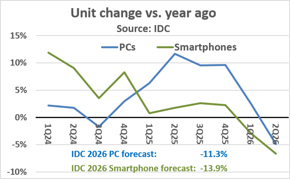
The current semiconductor memory boom is mainly an AI-driven capacity-allocation problem, not simply a lack of factories.
AI accelerators require enormous quantities of high-bandwidth memory, or HBM. HBM is used alongside GPUs and custom AI chips because it can move data much faster than ordinary server memory. As companies… Read More


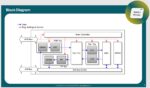


Enhancing Multi-Domain System Simulation with FMI Co-Simulation