You are currently viewing SemiWiki as a guest which gives you limited access to the site. To view blog comments and experience other SemiWiki features you must be a registered member. Registration is fast, simple, and absolutely free so please,
join our community today!
With each new silicon process node, the complexity of SoC design rules and physical verification requirements increases significantly. The foundry and an EDA vendor collaborate to provide a “reference flow” – a set of EDA tools and process design kit (PDK) data that have been qualified for the new node. SoC design methodology … Read More
In the EDA space, nothing seems to be more fragmented in-term of solutions than in the Design Verification (DV) ecosystem. This was my apparent impression from attending the four panel sessions plus numerous paper presentations given during DVCon 2018 held in San Jose. Both key management and technical leads from DV users community… Read More
The time is 1995 and my mandate as Layout Manager is to grow my team. I advertised everywhere but there were no experienced people in Canada that I can hire so the solution was back to training. I was the trainer a few times in Israel in MSIL but there we had a very organised material for layout, UNIX, software, etc. We had exercises, tests,… Read More
Thanks to my growing involvement in formal (at least in writing about it), I was happy to accept an invite to this year’s Oski DVCon dinner / Formal Leadership Summit. In addition to Oski folks and Brian Bailey (an esteemed colleague at another blog site, to steal a Frank Schirrmeister line), a lively group of formal users attended… Read More
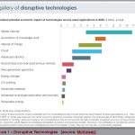
The semiconductor industry has gone through several major transitions driven by different dynamics such as shift in business models (fab-centric to fab-less), product segmentation (system design house, IP developers) and end market applications (PC to cloud; and recently, to both automotive and Internet of Things — IOT’s,… Read More
On LinkedIn I have some 2,116 connections and many of those are students looking to enter the field of EDA, IP or semiconductor design. What a wonderful opportunity these students have by attending the 55th annual DAC in San Francisco this summer from June 24-28. Technical sessions, keynote speeches, exhibitors, networking, … Read More
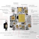
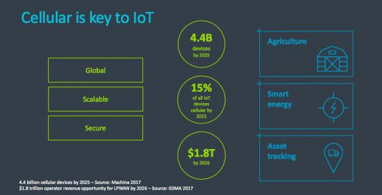
It seems that a hot ticket at Mobile World Congress this year was embedded SIM announcements. As a reminder of why this space is hot, cellular communication for provisioning and data uploads is a very real option for many IoT devices. In agricultural, smart energy and asset tracking applications for example, near-range options… Read More
There is a bit of nostalgia here since ClioSoft was one of the first companies that we (SemiWiki) worked with 7 years ago. Back then it was hard for an emerging EDA company to get noticed by the mainstream media much less collaborate with them. Since then we have published 80 blogs with ClioSoft that have garnered more than 350,000 views.… Read More
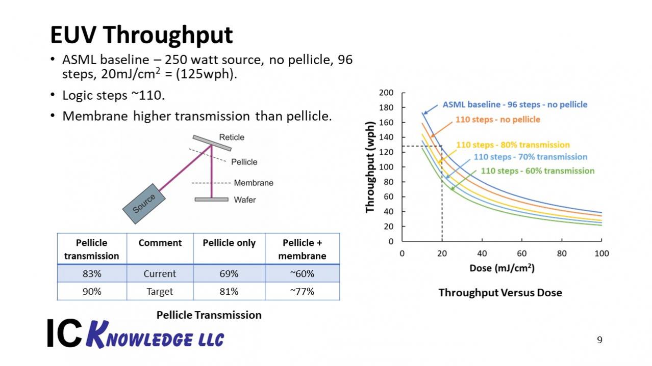
This year the Advanced Lithography Conference felt very different to me than the last couple of years. I think it was Chris Mack who proclaimed it the year of Stochastics. EUV has dominated the conference for the last several years but in the past the conversation has been mostly centered on the systems, system power and uptime.
I … Read More
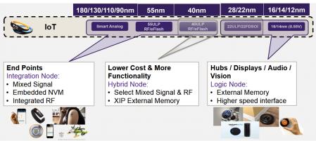
The projected revenue growth rate for IoT electronics remains strong, across a wide range of applications – e.g., visual object identification, voice recognition, machine automation, health and fitness applications, environmental and energy controls. A key component of these designs is the analog-to-digital conversion… Read More


Musk’s Orbital Compute Vision: TERAFAB and the End of the Terrestrial Data Center