The time is 1995 and my mandate as Layout Manager is to grow my team. I advertised everywhere but there were no experienced people in Canada that I can hire so the solution was back to training. I was the trainer a few times in Israel in MSIL but there we had a very organised material for layout, UNIX, software, etc. We had exercises, tests, some senior people as teaching assistants, a flow. I knew what is needed so I started developing everything. From testing aptitudes and teaching materials, from schematic for cells and blocks with progressive complexity, all had to be invented and generated from scratch. We had a layout team of 5 people and needed to double that so everybody joined to help. We did it and all the students are still successful in Layout 20+ years later. If you want to know more about this read our next book revision coming out before theend of 2018. After so many training classes I was really tired to repeat myself and wanted a better solution. The idea that a book may help started to grow in my mind. I started to talk to layout schools in US, IBT, Gered, etc., and received their curriculum’s. Some enthusiastic instructors like Dan Asuncion just shared with me their training class materials. I inquired with my former team in MSIL, so Zehira Dadon-Sitbon, the layout manager at that time, helped me reinvent the aptitude test. I got a lot of materials from all over the world but the table of content for “the book” was still far from comprehensive to the level I wanted. Many questions needed answers and nobody around could help. I did not know what is needed to write a book at that time.
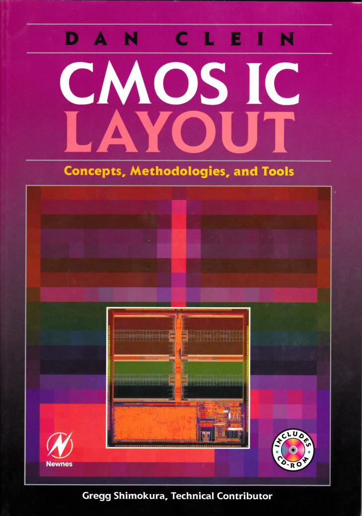
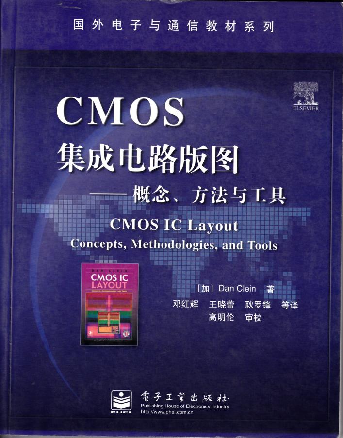
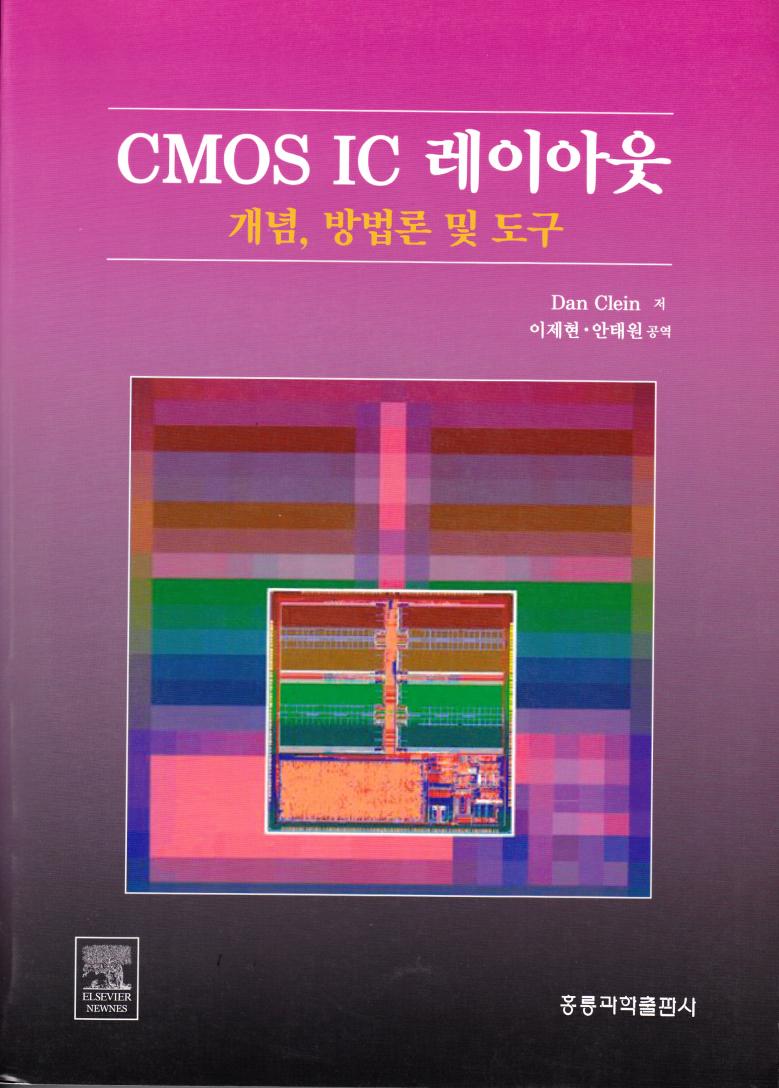
To put a little gas on the fire when I asked IEEE if they are interested to publish a Layout book they told me that if such book does not exit, it means its not needed!!! How wrong they proved to be… Check the attached pictures of a layout book translated in Chinese and Korean.


I was determined to move forward but I needed help and luckily it came from a work colleague. Gregg Shimokura, a Design Engineer who decided that MOSAID needs a CAD group so he built one, volunteered to help me. The starting point was our internal training course but we did not know if this is good enough for a book. Opportunity came to us as MOSAID was interested to increase the number of engineers with Memory expertise in Ottawa. They invited Carleton University professors for an internal DRAM course that was meant to be the base for a Memory course in University. This was my occasion to talk to Tad Kwasniewski (who passed away in February 2018). I wanted to know his thoughts: can such book be of interest for his university curriculum? After some research he came back with a solution: I will prepare a course of VLSI introduction for master students and teach at Carleton and this way I can test my material viability live. Based on Tad guidance, in 1996 I worked with Martin Snelgrove for VLSI Design course fall sessions. He was teaching Circuit and I was teaching Layout. The course was so successful that they invited me back but Martin wanted to move to Toronto so I needed a front-end person to teach Design. Like a real partner, Gregg jumped on this opportunity and together we taught VLSI Design 97.584 course at Carleton, fall 1997. We worked full time in MOSAID (!) and we worked nights and weekends to prepare materials and print them on overhead transparency film before each class (we invented Just In Time). Twice a week we were in class in front of 44 students for 3 months. At the end of the term we had to invent an exam, not a multiple-choice but with real solutions, in 2 versions, including design and layout. We were lucky we had 2 good TAs. One of them Rolando Ramirez Ortiz worked with me in PMC Sierra later.
Using the lessons learnt and the course materials, using a few other schools training materials we started to write the book.
In 1998 Gregg Shimokura and myself finished to write our book, CMOS IC Layout Concepts, Methodologies and Tools. We sent the manuscript to editors and worked with them on all implementation details. With more than 150 VISIO graphics and about 200 pages of text this was a gargantuan effort. We worked about 2000 hours on this, this is 6 months extra work for each of us, in top of our daily jobs! But the book came out in Dec 1999 and we became famous!
How is this for a NON “polygon pushing” assignment?
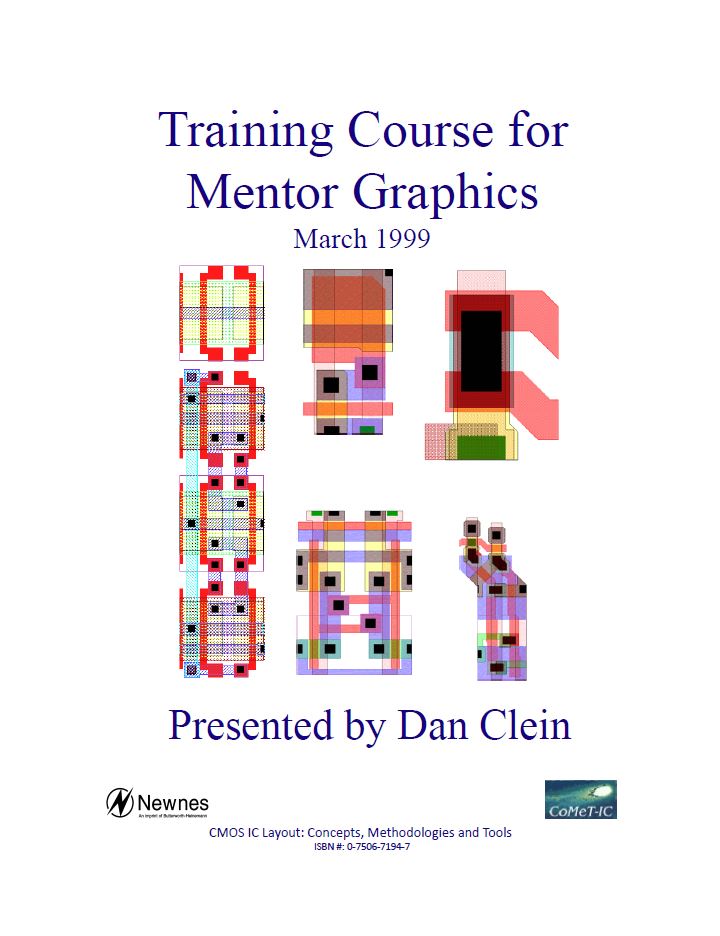
Last important “non-layout” activity in MOSAID was a training course for Mentor Graphics AEs and internal software developers. MOSAID decided at that time that from Design Services for Memories it’s time to extend into products with memory inside, meaning we wanted to go into ASIC. Suddenly we needed a lot of people trained in all Digital Design activities. Mentor had a good set of training courses and we decided to use them but no budget for it. Gregg Shimokura and myself just finished the manuscript for the first edition of our book. Thinking “outside the box” Roger Colbeck, our VP and Dan Chapman, Mentor Graphics account manager came up with a proposal. Knowing that we finished our book manuscript maybe Gregg and I can transform our book in a 5 days training course and exchange this for a digital training course for our engineers. We worked hard for a few weeks (again) to create the training classes in PowerPoint slides, print the materials and put them in booklets. Then I organized the trip and classes with Janet (Scheckla) Petersen, marketing manager in Mentor at that time and I travelled to Wilsonville. It was a tremendous experience to learn from participants what are the challenges of internal EDA teams. It’s difficult to understand what a USER wants/needs from a document written by a technical marketing person without ever meeting a customer. Most of them never did layout or circuit design so it was an eye opener on both sides. Was very useful for my growth to learn from AEs what are their challenges when working with customers. I was on the other side of the wall! Afterwards when a tool did not do what expected I was able to “imagine” the reasons why there is a difference between the manual and tool performance and adjust my expectations. I became able to relate to developers and help them modify the tools to make them more user friendly. I gained lot of friends in the EDA industry and found out that I like training again.

More to come while I worked in the next company…
Dan
Also read: Is there anything in VLSI layout other than “pushing polygons”? 1-6
Share this post via:


Solving the EDA tool fragmentation crisis