With the increasing density of electronics in product enclosures, combined with a broad range of operating frequencies, designers must be cognizant of the issues associated with the radiation and coupling of electromagnetic energy. The interference between different elements of the design may result in coupling noise-induced… Read More
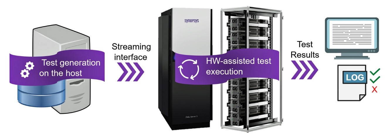
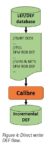
GDS and LEF/DEF each came about to support data exchange in different types of design flows, custom layout and place & route respectively. GDS (or stream format) was first created in the late 1970s to support the first generation of custom IC layout tools, such as Calma’s GDSII system. Of course, the GDS format has been updated… Read More
Last August I detailed a webinar about HCL Compass, a tool that provides low-code/no-code change management capability for enterprise scaling, process customization and control to accelerate project delivery and increase developer productivity. There is a lot of activity these days to migrate various enterprise applications… Read More
-Intel good results had a little extra help to be great
-New CEO commits to remaining an IDM versus fabless
-Claims of strong progress on 7NM fuel optimism inside
-Outsourcing to TSMC will not go away but will increase
A good quarter but with some silicon enhancements from ICAP
Intel reported Revenues of $20B and EPS of $1.52, which… Read More
A study published in ScienceAdvances has shown computer simulations of the movement of virus-laden airborne droplets in cars. The objective of the study appears to be to assess the degree of driver-to-passenger and passenger-to-driver exposure given different open-or-closed window configurations in the context of modeled… Read More
– ASML has good quarter driven by DUV & Logic (@72%)
– SMIC & other major customer slow EUV plans
– Logic (read that as TSMC) remains key demand led driver
– We are happy memory remains muted given cyclical potential
A very solid quarter with a continued road to growth
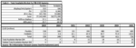
The quarter came in at Euro4,254B… Read More
Dan and Mike are joined by industry expert Robert Maire for a discussion on China based semiconductors. Robert is an internationally recognized expert on all aspects of semiconductor manufacturing. He joined SemiWiki in 2015 and his blogs have garnered more than 2 million views and many pointed discussions. Robert founded Semiconductor… Read More
Lee-Lean Shu co-founded GSI Technology in March 1995 and has served as President and Chief Executive Officer and as a member of the Board of Directors since its inception. In October 2000, Mr. Shu became Chairman of the Board of GSI Technology. Mr. Shu was has held various management positions in SRAM and DRAM designs at Sony Microelectronics… Read More
Smartphone shipments have been dropping over the past few years, as shown in Chart 1, as a result of several factors, but primarily the slowdown in smartphone innovation while at the same time prices have kept increasing. Even with the much anticipated 5G in 2020, unimpressive speed gains coupled with a Covid-19 backdrop, smartphones… Read More


Why Huawei Says It Will Match TSMC’s Most Advanced Chips by 2031