

Dr. Moh Kolbehdari is a Senior Lead Architect at Socionext, where he specializes in the industrialization of high-performance AI chiplets and 1.8-Tb/s interconnects. With over two decades of experience in SI/PI, electromagnetic field theory, and system-level architecture, he has been a pivotal force in bridging the gap between cutting-edge silicon design and high-volume manufacturing (HVM).
Dr. Moh is the creator of the SEGA™ (Systematic Engineering Governance Architecture) framework, a methodology designed to solve the “Crisis of Complexity” in heterogeneous integration. His work focuses on transforming the package into an Active Control Plane, utilizing field-confined EM Corridors and state-aware causality to ensure deterministic yield at 2nm and beyond. He is a frequent contributor to industry-standard committees and is recognized for his “Physics-First” approach to solving the semiconductor industry’s most challenging entropy walls.
The Entropy Wall at 2nm
The semiconductor industry is hitting a “Traceability Wall”. As we push toward 1.8-Tb/s interconnects and massive 2.5D/3D AI chiplet systems, the traditional design-then-verify flow is breaking down. We can no longer afford to treat the package as a passive “container” for silicon; at these speeds and densities, the package must be viewed as the Active Control Plane.
The “Reality Gap”—the delta between golden-state simulations and high-volume manufacturing (HVM) yield—is widening. Standard EDA tools excel at predicting nominal performance, but they often fail to account for the stochastic nature of the OSAT environment. To close this gap, we must move beyond “Nominal Design” and embrace Governed Convergence.
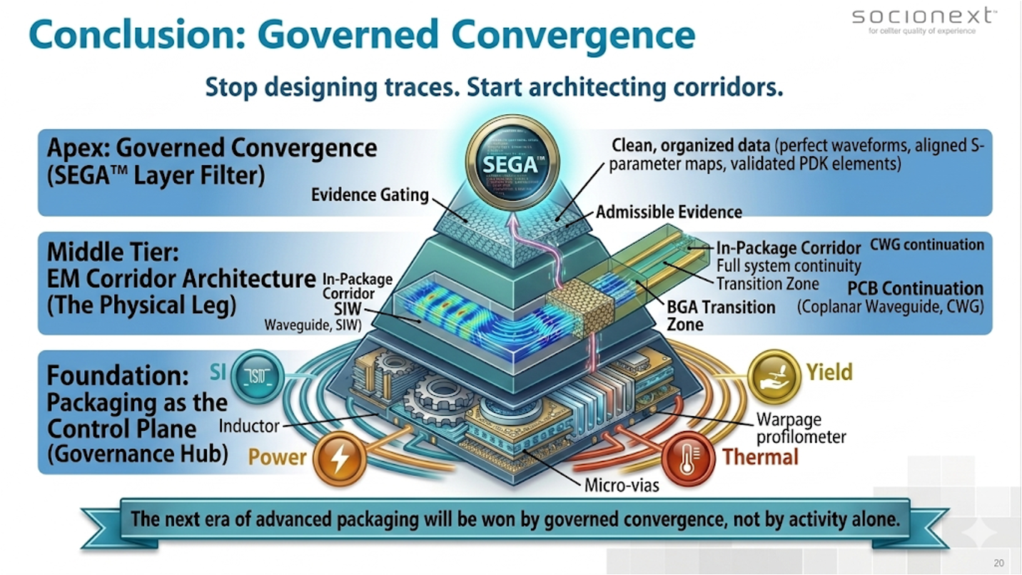
Introducing SEGA™: Systematic Engineering Governance Architecture
To address this complexity, I have developed SEGA™. It is a governance layer that sits above the standard EDA ecosystem, enforcing a unified “Readiness Loop” between simulation, lab measurement, and OSAT metrology. SEGA™ ensures that every picosecond of signal performance is backed by admissible evidence from the assembly floor.
")
As shown in the pyramid, SEGA™ establishes a three-tier hierarchy for system success:
- The Foundation: Packaging as the Control Plane. This tier treats the substrate as a dynamic hub that governs the convergence of SI, PI, Power, and Thermal stresses. By managing these variables in a unified hub, we prevent late-stage design “blow-ups” that typically occur when these domains are siloed.
- The Middle Tier: EM Corridor Architectures. Traditional PCB and package traces rely on “dirt road” routing that becomes chaotic at sub-THz frequencies. We implement field-confined physical pathways—EM Corridors—that ensure electromagnetic field continuity across the BGA transition zone.
- The Apex: Evidence Gating. This is the final filter. Only data that passes the State-Aware Causality filter is allowed to proceed to tape-out. This means every simulation result must be “certified” against known physical manufacturing modes.
Confronting the OSAT Reality
The biggest threat to modern chiplet systems isn’t just signal decay; it is the physical variables of the assembly floor. Substrate warpage, solder-bump collapse, and thermal drift create an OSAT Reality that golden simulations often ignore. When a design moves from the lab to HVM, these physical stresses introduce “entropy” that degrades performance.
")
By using State-Aware Causality, we link performance decay directly to specific deformation modes. For example, if a 1.8-Tb/s eye diagram closes during stress testing, the SEGA™ framework doesn’t just report a failure; it tells us exactly which manufacturing variable—such as a $30\mu$m substrate warp or lateral misalignment—caused the shift. This transforms “failure analysis” from a reactive guessing game into deterministic governance.
Deep-Dive Case Study: AI Chiplet PDN Impedance Flattening
The power of systematic governance is most visible in the Power Delivery Network (PDN). In high-performance AI systems, suppressing mid-frequency die resonance is critical for maintaining system stability under heavy workloads.
")
Our case study on 2.5D AI Chiplet Power Architecture (CPA) demonstrates how implementing a Localized VRM (PCA) governs the PDN. Traditionally, VRMs placed on the PCB struggle to manage the resonance peaks occurring at the interposer and die levels. By aligning the VRM response directly with the in-package parasitics discovered via our state-mapping, we successfully suppressed the die resonance peak (occurring between 170–280 MHz) to remain consistently below the $0.09 \Omega$ Target.
This level of flattening ensures that the silicon sees a stable voltage environment regardless of the switching activity of adjacent chiplets. This is a result that “golden” simulations can suggest, but only a governed architecture like SEGA™ can guarantee in a mass-production environment.
The Path Forward: Industrializing the Interconnect
The move toward 2nm and beyond is not just a lithography challenge; it is a governance challenge. As we move toward 10 Tb/s UCIe targets and increasingly complex heterogeneous systems, the architects who can bridge the gap between simulation and the factory floor will define the future.
The next era of advanced packaging will be won by governed convergence, not by activity alone. By implementing SEGA™, we move the industry toward a future where “first-time-right” isn’t a goal—it is a deterministic outcome of the architecture itself.
Also Read:
Alchip’s Leadership in ASIC Innovation: Advancing Toward 2nm Semiconductor Technology
Synopsys Advances Hardware Assisted Verification for the AI Era
Scaling Multi-Die Connectivity: Automated Routing for High-Speed Interfaces
Share this post via:


The Semiconductor Growth Numbers are Insane but the Real World Doesn’t Tally!