You are currently viewing SemiWiki as a guest which gives you limited access to the site. To view blog comments and experience other SemiWiki features you must be a registered member. Registration is fast, simple, and absolutely free so please,
join our community today!
At Intel we mused about designing wafer-scale integration (WSI) back in the 70’s however I just learned about how Dr.Renato Turchetta at the Science and Technology Facilities Council (STFC) designed a wafer-scale imaging sensor chip for X-Ray applications. I was also able to interview Dr. Turchetta to learn more about… Read More
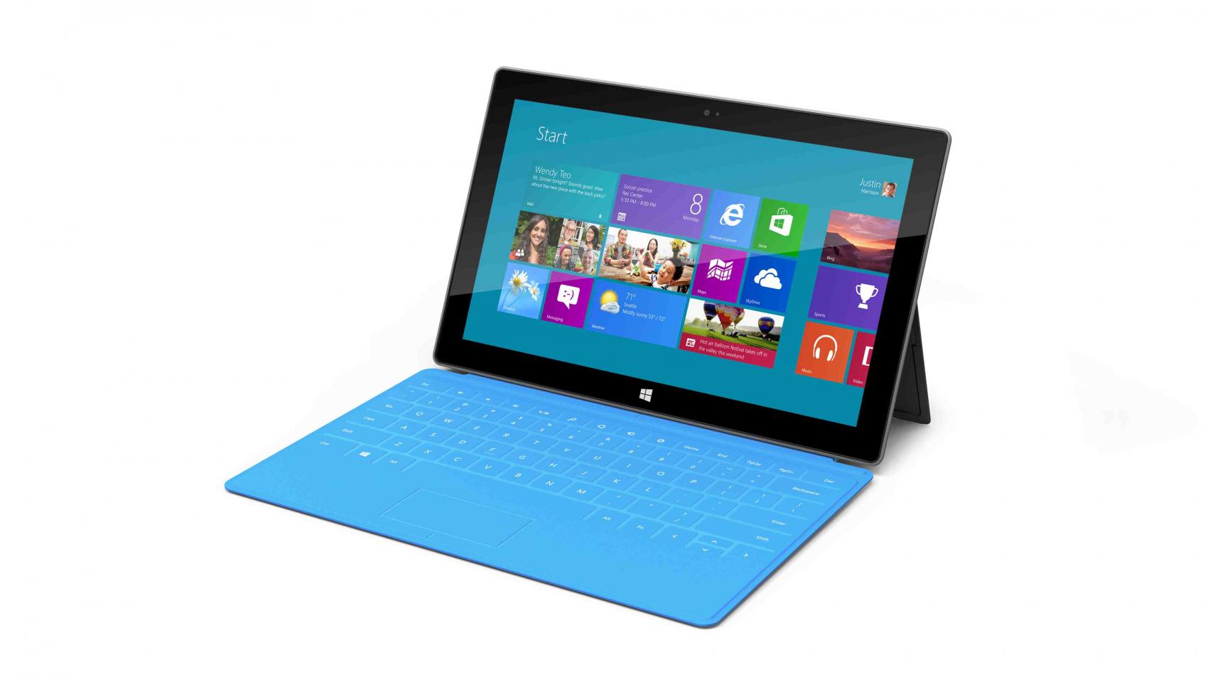
Microsoft is in trouble. Many of you already know that. Steve Ballmer has one last opportunity to set the company on a growth path or they will retreat into IBM legacy mode… ala the post 1990s Lou Gerstner era. And so they introduce a large tablet-convertible in direct competition with their PC partners Dell and HP. The End Game is coming… Read More
I met with Amit Gupta, President and CEO of Solido at DAC on Tuesday to get an update on their EDA tools used in the design of memory, standard cells and low-power. In 2012 they’ve expanded to add three new software packages: Memory, Standard Cell, Low Power. They must be doing something right because at DAC this year I see more… Read More
Edmond Macaluso, President of Z-Circuit Automation met with me at DAC on Tuesday afternoon to provide an overview of how their EDA tools characterize cell libraries. … Read More
Mike Muller’s keynote focused on a lot of changes since the ARM1 was designed in 1983 when ARM the company did not exist and ARM was the next generation processor for Acorn Computer, which was really in the hobby market and had its first boost when they had a contract to design the BBC Microcomputer to go along with a computer literacy… Read More
Off topic: Mattby Paul McLellan on 06-20-2012 at 8:12 pmCategories: General
This has pretty much nothing to do with EDA or semiconductor. OK, absolutely nothing. Years ago a friend pointed me at a video of a guy who used to be a video game designer (wait, a semiconductor connection) who decided to take his savings and travel the world. As he put it, “I wasn’t a very good video game designer. But I … Read More
David Abercrombie from Mentor Graphics met with me on Tuesday at DAC to provide an update on DPT – Double Patterning Technology, something new required for several layers starting at the 20nm node in order to get any IC yield. DPT is also part of Multiple-Patterning.… Read More
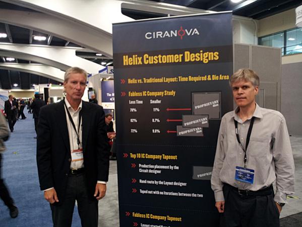
Three people from Ciranova met with me at DAC this year: Eric Filseth (CEO), David Millman (Marketing) and Lindor Hendrickson (CTO). They gave me an update on how the Helix tools are being used to automate the layout of custom IC designs at 28nm and smaller nodes.… Read More
IPL Alliance at DACby Daniel Payne on 06-20-2012 at 3:25 pmCategories: EDA, Synopsys
Lunch on Tuesday at DAC was sponsored by the IPL Alliance and thankfully this year they skipped the attempt at humor and focused on interoperable PDKs. Presenting companies include: Synopsys, Dongbu HiTek, TowerJazz, X-FAB and Si2. Having both OpenPDK and iPDK on the same platform does sound like a peaceful co-existence to me,… Read More
The Linley group is the go-to source for information about the microprocessor market. If you go back to their roots in Michael Slater’s Microprocessor Report then they have been in the business for 25 years. We haven’t had microprocessors for that much longer. They just tagged Tensilica as being second in shipments… Read More

















The silent killer of analog reliability: Why SPICE misses floating net