Array
(
    [content] => 
    [params] => Array
        (
            [0] => /forum/index.php?threads/tsmc-celebrates-as-arizona-hits-key-construction-milestone-on-second-fab.19692/
        )

    [addOns] => Array
        (
            [DL6/MLTP] => 13
            [Hampel/TimeZoneDebug] => 1000070
            [SV/ChangePostDate] => 2010200
            [SemiWiki/Newsletter] => 1000010
            [SemiWiki/WPMenu] => 1000010
            [SemiWiki/XPressExtend] => 1000010
            [ThemeHouse/XLink] => 1000970
            [ThemeHouse/XPress] => 1010570
            [XF] => 2021370
            [XFI] => 1050270
        )

    [wordpress] => /var/www/html
)

TSMC celebrates as Arizona hits key construction milestone on second fab!

Daniel Nenni

Admin
Staff member
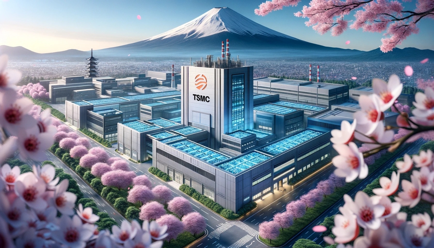
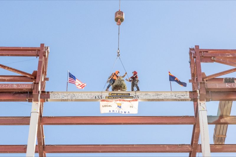
TSMC Arizona celebrated a “topping out” milestone today — signifying the last steel beam being raised into place on a construction project — for our second semiconductor fab in Phoenix, Arizona. We also recently achieved the topping milestone on our second fab’s auxiliary buildings, which will supply the necessary utilities infrastructure to the second fab clean room. We also continue to make significant progress completing our first fab which remains on track to begin production in the first half of 2025.

Once operational, our two fabs at TSMC Arizona will manufacture the most advanced semiconductor technology in the U.S., creating 4,500 direct high-tech, high-wage jobs and enabling our customers’ leadership in the high-performance computing and artificial intelligence era for decades.

Today’s ceremony was a momentous occasion for TSMC Arizona and our outstanding construction partners. TSMC Arizona CEO Y.L. Wang and President Brian Harrison joined the assembled trade workers and extended thanks for their hard work and valued craftsmanship. At the event, we were proud to stand alongside our important construction partners, including Austin Commercial, Baker Concrete Constructors, BUESING CORP, Rolling Plains Construction, and W&W|AFCO Steel.

#semiconductors #manufacturing #construction #phoenix #chips #innovation
Activate to view larger image,
No alternative text description for this image

Activate to view larger image,
No alternative text description for this image

Activate to view larger image,
No alternative text description for this image

Activate to view larger image,
No alternative text description for this image

Activate to view larger image,
No alternative text description for this image


Do some research on when this milestone was done in Phase 1. This was the easy stuff! All the complicated stuff comes after the building. This is nothing but a press event, says nothing about the challenges that TSMC faced and stumbled in Phase 1 and no indication that they have made any traction against those failures
 
This announcement is about the fab02 (or phase 2) building of TSMC's Phoenix project. The phase one building completed about a year ago and TSMC is in the process to install all the equipments.

See the site map below:

Thread 'TSMC Phoenix Arizona Fab Site Plan' https://semiwiki.com/forum/index.php?threads/tsmc-phoenix-arizona-fab-site-plan.16066/
you are correct. I am asking about the phase one. Phase two will ramp once the demand is there. So will phase one or Fab 52 ship wafers first?
 
you are correct. I am asking about the phase one. Phase two will ramp once the demand is there. So will phase one or Fab 52 ship wafers first?

From the progress of building construction itself, TSMC Phoenix Fab01 is ahead of Intel Phoenix Fab 52. In December 2022, TSMC hold a "First Tool-In" ceremony at Phoenix site wile Intel released a video to celebrate the first roof truss installation at Fab 52. But there are more factors critically impact the real HVM date at each fab. Some of those factors are beyond Intel or TSMC's control.

 
From the progress of building construction itself, TSMC Phoenix Fab01 is ahead of Intel Phoenix Fab 52. In December 2022, TSMC hold a "First Tool-In" ceremony at Phoenix site wile Intel released a video to celebrate the first roof truss installation at Fab 52. But there are more factors critically impact the real HVM date at each fab. Some of those factors are beyond Intel or TSMC's control.

First tool in December 2022 and Production in 2025. I did a quick search on the web and there is not even a clear date in 2025. It is already March 2024. Even the definition of milestone can be twisted. What does production really mean!

Those in the know pull out your planner. What is the milestone, Certified Production wafers start, out or what. To get to production out would mean 3 months to wafer starts, you have the pilot wafer starts, targeting. I would schedule some process window and anticipated issues and learning than the run thru the fab, package builds and reliability stress.

First tool in December 2022, assume the litho tools come in around that time, tool install, tool qual, matching module work, short loop run, full loop run and yield match and finally reliability ……. Hmmmm
 
Last edited:
During the 2022-12-06 ceremony (to celebrate the first batch of state of-the-art semiconductor manufacturing equipment to arrive in TSMC Arizona), TSMC revealed six semiconductor tools which are designed to support production of leading-edge semiconductor process technology. Among these include tools from long-time suppliers Applied Materials, ASM, ASML, Lam Research, KLA and Tokyo Electron.

15 months later...
 
@hist78 @milesgehm @TBiggs TSMC phase one will start wafers in 1H25. Intel Fab 52 is scheduled for 2H25. Correct? Intel has not started tool install in F52 correct?


First tool in December 2022 and Production in 2025. I did a quick search on the web and there is not even a clear date in 2025. It is already March 2024. Even the definition of milestone can be twisted. What does production really mean!

Those in the know pull out your planner. What is the milestone, Certified Production wafers start, out or what. To get to production out would mean 3 months to wafer starts, you have the pilot wafer starts, targeting. I would schedule some process window and anticipated issues and learning than the run thru the fab, package builds and reliability stress.

First tool in December 2022, assume the litho tools come in around that time, tool install, tool qual, matching module work, short loop run, full loop run and yield match and finally reliability ……. Hmmmm
 
Meanwhile TSMC readies manufacturing in Japan in 2 years versus 3 or 4. Amazing. Rumor has it Sony (investor) sped things along quite a bit. It has been dubbed the Nightless Castle since they worked around the clock to get it done.

TSMC Nightless Castle.jpg


Meanwhile TSMC readies manufacturing in Japan in 2 years versus 3 or 4. Amazing. Rumor has it Sony (investor) sped things along quite a bit. It has been dubbed the Nightless Castle since they worked around the clock to get it done.

View attachment 1733

I wonder if the major contractors or subcontractors or union at the Az site knows about commitment and honor and was willing to work one extra hour without OT pay .

Really why would anyone expect things in the US to go smoothly. Intel folks are well experienced but I doubt anyone at TSMC was willing to listen, CC talks about being humble from what I hear no one at Az was humble
 
Meanwhile TSMC readies manufacturing in Japan in 2 years versus 3 or 4. Amazing. Rumor has it Sony (investor) sped things along quite a bit. It has been dubbed the Nightless Castle since they worked around the clock to get it done.

View attachment 1733


The JSMC/TSMC site used three regular daily shifts during the building construction and four daily shifts to install the fab equipment. That's part of the many reasons why it can finish the fab, including the equipment installation, in 20 months. These kinds of approaches are probably so remote to US industry and labor unions.

The semiconductor industry is a global industry. No matter you like or not, the competition is coming from everywhere and going to everywhere. The features, quality, availability, and cost of the final semiconductor products will ultimately decide whether a welder, a chip design engineer, a nitrogen gas supplier, or a building custodian can compete against someone thousands miles away in another country.

While the general contractor of JSMC recruits workers all over the Japan to meet the fab project deadline, Arizona union workers expressed their displeasure that many cars on the TSMC Phoenix construction parking lots are with out of state license plates.
 
Last edited:
I wonder if the major contractors or subcontractors or union at the Az site knows about commitment and honor and was willing to work one extra hour without OT pay .

Really why would anyone expect things in the US to go smoothly. Intel folks are well experienced but I doubt anyone at TSMC was willing to listen, CC talks about being humble from what I hear no one at Az was humble
The article mentioned salaries for some of the work in Japan being 66% higher than nominal to entice workers. Sounds like even in Japan it takes more than appeals to honor to motivate the workers.
 
The article mentioned salaries for some of the work in Japan being 66% higher than nominal to entice workers. Sounds like even in Japan it takes more than appeals to honor to motivate the workers.
In Japan, people get high pay from doing financials/lawyers and the pay for tech workers are not so good. Hence it's relatively easy for JSMC to give Japan workers higher pay than market average.
 
In Japan, people get high pay from doing financials/lawyers and the pay for tech workers are not so good. Hence it's relatively easy for JSMC to give Japan workers higher pay than market average.
Sound like the US, just add doctors into the triumphant highly over compensated trio.
 
Meanwhile TSMC readies manufacturing in Japan in 2 years versus 3 or 4. Amazing. Rumor has it Sony (investor) sped things along quite a bit. It has been dubbed the Nightless Castle since they worked around the clock to get it done.

View attachment 1733

So this pic is a AI rendering of an interpretation of a cartoon????
 
Back
Top