You are currently viewing SemiWiki as a guest which gives you limited access to the site. To view blog comments and experience other SemiWiki features you must be a registered member. Registration is fast, simple, and absolutely free so please, join our community today!
TechInsights identified the MicroBT ASIC chip as the first commercialized product using GAA technology in the industry.
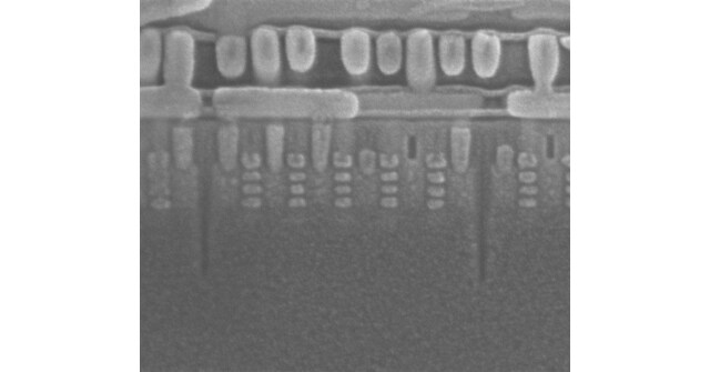
"Samsung claims its first-generation 3nm process could reduce power consumption by 45%, increase performance by 23%, and reduce chip area by 16% compared to 5nm technology, promising even more advances for future generations."
/PRNewswire/ -- Semiconductor industry research firm TechInsights said it has found that Samsung's 3nm GAA (gate-all-around) process has been incorporated into...
www.prnewswire.com
Design rules are still loose, as the comparison with 5nm indicates.
I don’t know what you mean by if true? They already disassembled the part and have TEMs. As for first commercially available GAA process; ehhhh let’s see an exyonos that has any analog or sram content rather than a couple thousand wafers of pure logic. If memory serves from the teardown and what bitcoin ASICs are; they are like 10-20 mm2 dies, consisting of repeating arrays of small logic functions, with no analog or sram content. It is also my understanding that these things have low performance/reliability requirements because all they care about is power per coin minted, and replacing these things with new die shrinks every couple of years to try and get a leg up on their competitors who all have identical ASIC designs. If we see an actual high volume product in at least the hundreds of thousands units range (rather than a lohihi 2 like ultra low volume part) then I am willing to dole out crowns to SF3E. Unfortunately it is looking like we and Samsung will have to wait for SF3 to get their first to GAA crown (hopefully for the spring 2024 phone refresh cycle as I’d love to see the evolution from SF3E).
"DIGITIMES Research semiconductor analyst Eric Chen pointed out that Samsung indeed has started producing chips using the 3nm GAA process, but the capacity is still small. "Getting revenues from shipment can be defined as 'commercialization', but ASIC is a relatively simple kind of chip to produce, in terms of architecture."
DIGITIMES analyst John Wang highlighted the fact that the yield of Samsung's 3nm GAA process is still low, so it will try to get as many customers as possible to help train its processes and improve the yield. It is understandable why they would do business with a Chinese customer."
SUMCO commenting on GAA on its Aug 8th earnings call. Presume by "well-known player" he means TSMC. later on the same call he said GAA 110 is quite tough & may happen 2025/26. GAA 100 is earlier. I dont know the diff between GAA100 and GAA110.
SUMCO commenting on GAA on its Aug 8th earnings call. Presume by "well-known player" he means TSMC. later on the same call he said GAA 110 is quite tough & may happen 2025/26. GAA 100 is earlier. I dont know the diff between GAA100 and GAA110.View attachment 1366View attachment 1367
Those are crystal orientations. Based on the whitepaper’s I’ve read the lowe mobility of that orientation is the root causes of GAA PMOS being much weaker than NMOS (relative to finFETs). By saying the orientation might change in the late 20s, he might be hinting that they are considering VTFETs or vertical nanosheets/wires in that timeframe. I think this because, I believe this is the only way to change the orientation like that (but mat sci is not something I’ve ever studied so I could be totally wrong).
SUMCO is raw wafer provider and I believe they are talking Si/SiGe superlattice layer stacking challenges, not device channel direction definition which is done in Fab side.
As I remembered, the requirement of layer composition transition between Si/SiGe need to be ~0.5nm which is ~ Silicon's lattice constant which could be very challenging.
What is 100 110 in reference too then if we are talking about wafer substrates? Is he talking about SiGe/different concentration SiGe stack like I’ve seen from some white papers from ROC universities?
What is 100 110 in reference too then if we are talking about wafer substrates? Is he talking about SiGe/different concentration SiGe stack like I’ve seen from some white papers from ROC universities?
When developing a new node with device performance and dimension/density targets(PPA) and more to meet, unless you can just follow the previous nodes to do modification, you need to consider thoroughly what will be device architecture, electrostatic performance, materials selection...., wafer substrate will be one of the key items. I believe here 100,110 are crystal plane orientations on wafer spec. The challenge had been discussed by one of epi tool supplier ASM in 2020, FYI.
How can intel 3 which is gonna be manufacturing ready this half of 2023 outperform TSMC 2N which will come out probably 1.5 to 2 years later? This means Samsung and TSMC can only catch up to Intel 3 by mid 2026 and by that time Intel increases the edge further with 18A. Is this even possible or is the roadmap unrealistic for intel?
How can intel 3 which is gonna be manufacturing ready this half of 2023 outperform TSMC 2N which will come out probably 1.5 to 2 years later? This means Samsung and TSMC can only catch up to Intel 3 by mid 2026 and by that time Intel increases the edge further with 18A. Is this even possible or is the roadmap unrealistic for intel?
This is obviously preliminary data in the chart, but a few items:
1. TSMC’s N2 is not going for performance or density crowns - it’s primary focus is to put GAAFETs into production so scaling and further improvements can continue after N2. Reduce risk to make GAAFETs work.
2. Intel is definitely giving up density to get the extra performance. This is not unusual in this field - if you look at some of Intel’s past processes, as clock speeds go up with iterations of a process node (i.e. 14+++ vs 14), the transistors actually get a little larger or take up more space (less density).
3. Intel generally has more of a bias towards performance than density vs. TSMC; and that’s because their own internal products benefit greatly from the additional frequency and other performance headroom’s.
How can intel 3 which is gonna be manufacturing ready this half of 2023 outperform TSMC 2N which will come out probably 1.5 to 2 years later? This means Samsung and TSMC can only catch up to Intel 3 by mid 2026 and by that time Intel increases the edge further with 18A. Is this even possible or is the roadmap unrealistic for intel?
Because Intel has always been the performance crown, which is the same reason AMD tends to have a hard time competing with Intel in single threaded performance.
The chart is showing Intel has a superior advantage in performance, whereas TSMC wins in terms of density. Their leadership positions in various segment are either continue or grow stronger.
I think it is totally possible. Intel has been late to EUV, Intel 3 is the second generation after they adopted EUV. But ASML has been helping them during COVID with all its technician with knowledge/experiences they learned from by collaborating with TSMC. ASML has the firsthand knowledge to help Intel out and they definitely want Intel to succeed so they can sell more equipment. TSMC is dealing not with China that has forbidden access to the most cutting-edge equipment, talent and material in the world. It is dealing with Intel that has all the helps from western countries, from IBM that has shared its research knowledge with Intel when it comes to leading edge process node. I believe there are still plenty of room for them to continue to deliver better transistors.
I think this is the type of technology know-how (or trade secret) leakage TSMC should have taken precautions against, in dealing with vendors such as ASML, or customers such as Intel. It is worse risk with Intel, who in effect forces TSMC to compete with its customer.
I think this is the type of technology know-how (or trade secret) leakage TSMC should have taken precautions against, in dealing with vendors such as ASML, or customers such as Intel. It is worse risk with Intel, who in effect forces TSMC to compete with its customer.
Not exactly. If TSMC said "Hey our tools are busted or we are having a hard time patterning x feature, fix it since we have no clue how." (which is to be expected from something that is new). Then any solution to that problem is ASML IP, not TSMC IP. Same thing with any modifications or upgrades ASML made from watching how TSMC's tools performed.
Not exactly. If TSMC said "Hey our tools are busted or we are having a hard time patterning x feature, fix it since we have no clue how." (which is to be expected from something that is new). Then any solution to that problem is ASML IP, not TSMC IP. Same thing with any modifications or upgrades ASML made from watching how TSMC's tools performed.
I think that argument only works for generic or vanilla lithography tasks, where the specs are somewhat loosened. There is still the influence of work or fab operation procedures such as wait time management, which will subtly affect chance of yield success.
We see publications by Samsung and Intel on their work with EUV, not really mentioning ASML as co-author. Why doesn't TSMC do the same? They probably want to keep some secrets.

 www.prnewswire.com
