
I plucked this quote from an IEEE article:
“Intel used to be the conservative one,” says Dan Hutcheson, vice chair of TechInsights. Previously, TSMC was more aggressive in its risk-taking, and the company more frequently missed the mark. Now, the situation has flipped, Hutcheson explains. “It’s a very risky move to try to implement two major technology changes at once, and in the past this has often been a recipe for disaster,” he says.
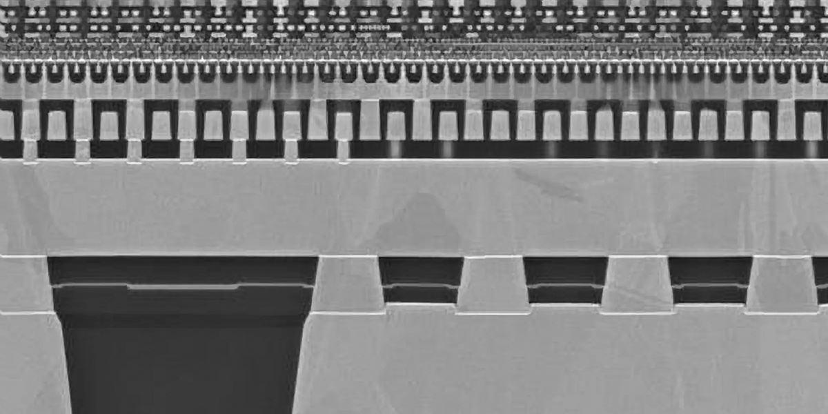
He is talking about Intel 20A with backside power delivery (BPD). I never considered TSMC a risk taker. They have customers to serve and their corporate lives depend on it (Trusted Foundry) . Examples: TSMC split double patterning at 20nm with FinFETs at 16nm. TSMC added EUV layers to 7nm (7nm+) after it was in HVM. That is not aggressive risk-taking, my opinion.
Intel on the other hand serves itself with internal developed products that can and have been delayed due to process issues. Intel risked doing double patterning and FinFETs at 14nm and did quite well. It was done in a stealthy manner so we do not know about delays and such but it was a very disruptive move. Intel risked doing 10/7nm without EUV and failed badly. For Intel the difference is that now they have competitive pressure at the product (AMD) and process (TSMC) level which they did not have before.
I also disagree with the quote about 20A with BPD being a risky move. Intel is bringing 20A to HVM then adding backside power delivery. Same with 18A, you are not required to do backside power delivery. Intel 18A stands on its own as an innovative process that is competitive with TSMC N2 and Samsung 2nm, even beating them to market. With backside power delivery Intel leap frogs ahead until TSMC and Samsung delivers BPD it a year or two later.
Correct me if I am wrong here but that quote in the context it was presented is nonsense.
 spectrum.ieee.org
“Intel used to be the conservative one,” says Dan Hutcheson, vice chair of TechInsights. Previously, TSMC was more aggressive in its risk-taking, and the company more frequently missed the mark. Now, the situation has flipped, Hutcheson explains. “It’s a very risky move to try to implement two major technology changes at once, and in the past this has often been a recipe for disaster,” he says.
He is talking about Intel 20A with backside power delivery (BPD). I never considered TSMC a risk taker. They have customers to serve and their corporate lives depend on it (Trusted Foundry) . Examples: TSMC split double patterning at 20nm with FinFETs at 16nm. TSMC added EUV layers to 7nm (7nm+) after it was in HVM. That is not aggressive risk-taking, my opinion.
Intel on the other hand serves itself with internal developed products that can and have been delayed due to process issues. Intel risked doing double patterning and FinFETs at 14nm and did quite well. It was done in a stealthy manner so we do not know about delays and such but it was a very disruptive move. Intel risked doing 10/7nm without EUV and failed badly. For Intel the difference is that now they have competitive pressure at the product (AMD) and process (TSMC) level which they did not have before.
I also disagree with the quote about 20A with BPD being a risky move. Intel is bringing 20A to HVM then adding backside power delivery. Same with 18A, you are not required to do backside power delivery. Intel 18A stands on its own as an innovative process that is competitive with TSMC N2 and Samsung 2nm, even beating them to market. With backside power delivery Intel leap frogs ahead until TSMC and Samsung delivers BPD it a year or two later.
Correct me if I am wrong here but that quote in the context it was presented is nonsense.
In 2024, Intel Hopes to Leapfrog Its Chipmaking Competitors
The chipmaker is betting on new transistors and power-delivery tech
spectrum.ieee.org