You are currently viewing SemiWiki as a guest which gives you limited access to the site. To view blog comments and experience other SemiWiki features you must be a registered member. Registration is fast, simple, and absolutely free so please, join our community today!
Well yeah. I was just using it for perspective, to remind people that back at that time EUV was NOT essential. The meme today "Intel forgot to use EUV, hence trouble" is what I was getting at.
10nm may have had weird pitch gearing. Intel 4 has lovely gearing combined with COAG, and is even dreamier with BSPD (even though that was just a demo process combined with 4). Indeed, IMO the metal/contact improvements are the heart of Intel 4, transistor size change seems mainly just fin count reduction and single diffusion breaks, not lithographic size.
I'm surprised you say this. Practically their whole product stack is intel 7 at this point. Considering the die sizes of the products there is no way the yield can be bad with how many units they can churn out and the margins intel had before the current downturn. Intel has also been very upfront with intel 4 being their first production application of EUV and that 10nm was not designed to cut in EUV.
Well yeah. I was just using it for perspective, to remind people that back at that time EUV was NOT essential. The meme today "Intel forgot to use EUV, hence trouble" is what I was getting at.
Fair enough. People forgetting N7 used optical only is also irksome to me as well. IMO this fallacy also devalues how well targeted N7 was. Right at the limits of SALELE with the option to insert limited EUV to derisk N5.
10nm may have had weird pitch gearing. Intel 4 has lovely gearing combined with COAG, and is even dreamier with BSPD (even though that was just a demo process combined with 4).
That is quite the glowing endorsement. From the perspective of random low level etch engineer it looks pretty ordinary. But I also know almost nothing about std cell architecting, so if there is something I am missing I'm all ears. Doubly so with your BSPD comment. What about the current metal gearing is great for that?
Indeed, IMO the metal/contact improvements are the heart of Intel 4, transistor size change seems mainly just fin count reduction and single diffusion breaks, not lithographic size.
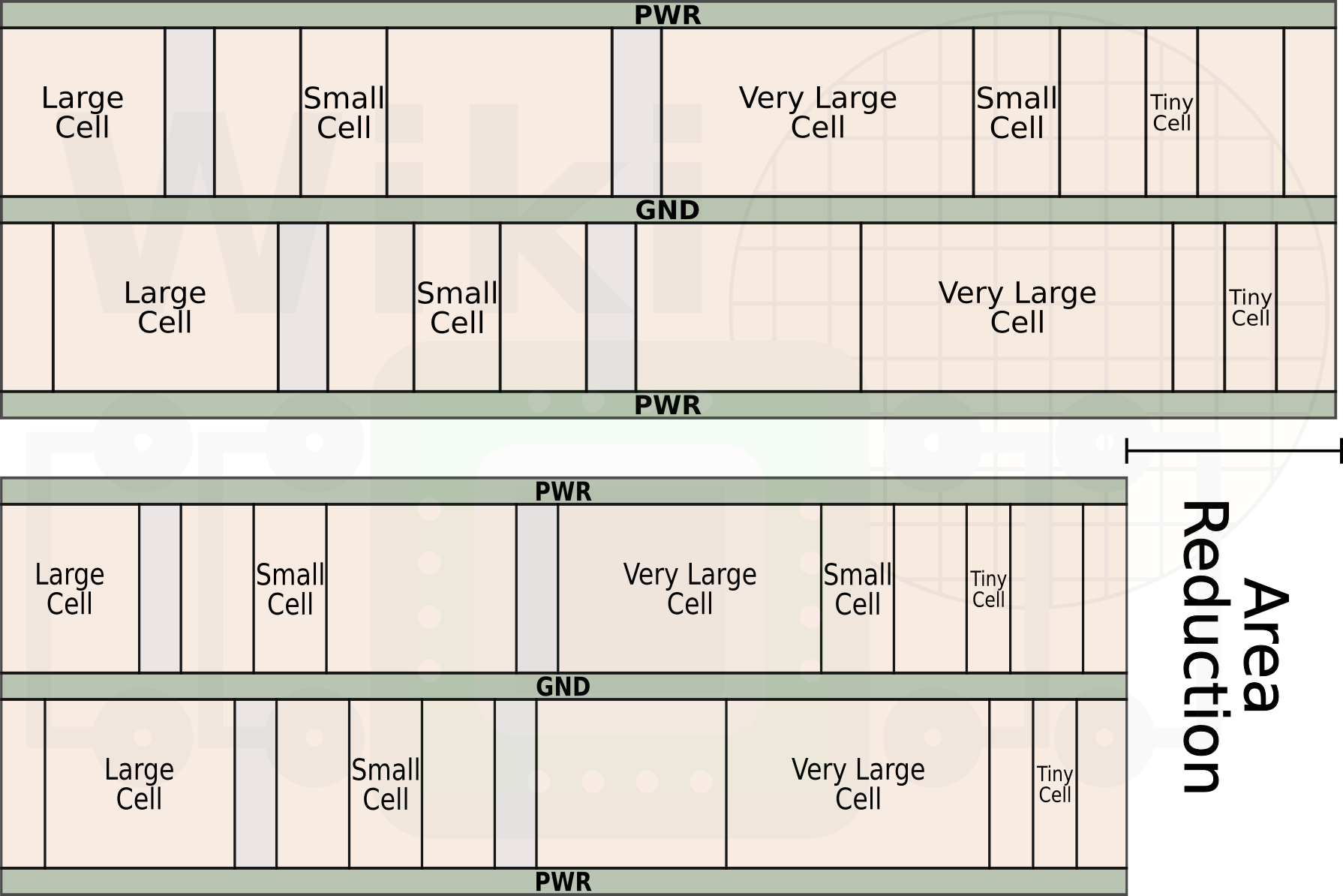
The ratio of m0 and M1 to the underlying features. To a first order, simply tighter pitch is better, but there are also issues like how it connects. Intel 7 (fka 10) had 3 fins for every 2 M0 and also some constraints on where the M0 could contact the gate metal. Intel 4 allows M0 to contact on top of gate (ie. fin location) and the M0 pitch is same as fin pitch. I don't know what the M1 metal pitch was in 10. The Intel 4 orthogonal M1 and M3 (and M5) pitch is 50nm, same as CPP and I assume they are aligned over the gates.
This is not just more ways to connect, but more freedom how to connect to the gate. When I experimented manually with this layout it means a lot of basic cells need only M0, at XOR level you need a bit of M1, and it was not until I got to a full adder that I needed M2. M2 has a 45nm pitch - 2 M2 per 3 fins which is also a bit wonky since it is not a divisor of the 240 nm track height. This makes it a little odd in basic cell design since the available geometry repeats only every 6 tracks (45nm divides into 3 tracks, but then you have Vdd and Vss inverted, so 6 tracks brings you back to isomorphic). I'm surprised they don't just use 48nm.
When you go to BSPD you get back one M0 track that used to be used for either Vdd or Vss, depending on how you look at it, but also some M0 pathways that were blocked for keepouts where the power vias came down. So I expect Intel 3 with 2 fins per transistor and BSPD will be about as easy to route at the cell level as Intel 4 with 3 fins per transistor. Of course, Intel 3 will still be more crowded for routing between cells, but the lack of keepouts around tall power vias should help, too. And the freedom to add power connects nearly everywhere with immediate transition to bigger metal should reduce droop improving low voltage operating margins.
You work with FF16, don't you have similar pitch rules there? When you get down to 7 and below I assume you can no longer play tricks like sequential gates without intervening source/drain contacts (i.e. naive multi-gate channels might not be allowed) so maybe some of these constraining rules are more important at smaller size.
Thanks. So "pitch gearing" is adjusting to for an unsynchronized pitch. I've never accessed rules below 12nm. We do need to be creative on TS 16-12 and GF14.
The ratio of m0 and M1 to the underlying features. To a first order, simply tighter pitch is better, but there are also issues like how it connects. Intel 7 (fka 10) had 3 fins for every 2 M0 and also some constraints on where the M0 could contact the gate metal. Intel 4 allows M0 to contact on top of gate (ie. fin location) and the M0 pitch is same as fin pitch. I don't know what the M1 metal pitch was in 10.
Presented at the 64th IEEE International Electron Devices Meeting (IEDM) in December, here's a look at Intel's 10-nanometer standard cell library and power delivery system.
fuse.wikichip.org
While looking for the explanation for why intel made the unusual choice of 36nm M1, I found one interesting nugget that I didn't know. That all 10nm std cells have a 7-track M0 arrangement. As the CH increased they would just increase metal pitch while keeping the arrangement the same. Seems really weird, but that might just be a byproduct of how pitch quartering works. IF SAPQ was the reason they did that arangment, I wonder why it is 7 tracks per cell and not 5 like the bellow example would indicate?
The A B A B A B A B .. pattern is endless, that makes the patterning extremely uniform and reliable. Deciding how to group them into tracks is quite separate.