You are currently viewing SemiWiki as a guest which gives you limited access to the site. To view blog comments and experience other SemiWiki features you must be a registered member. Registration is fast, simple, and absolutely free so please, join our community today!
But remember UMC is a for profit business. UMC is in no hurry to help a competitor or a future competitor, Intel. The agreement must come with other significant incentives to UMC.
Of course UMC wants to profit from this. My point was mostly centered on opportunity cost. UMC has very limited capex and R&D dollars. If they wanted to do this alone the scale of this 12nm node, the time it will take them to get there, and or the resources/capital from other programs would need to take a hit. Given their TD track record (ie needing to rely on the common platform alliance) UMC doing this by themselves would probably be slower, might have worse PPA, while also forcing UMC to eat the opportunity costs of not focusing on their core competencies when those can instead be footed by intel. I guess it depends on how the deal is set up... but if it is a cut of what IFS makes, then UMC also has one less fab to worry about filling. As for intel being a competitor they kind of are and aren't. UMC is more or less stuck on planar with alot of their capacity being on 200mm fabs. Meanwhile intel is stuck on 300mm finFET and beyond. Unless you count the tower deal intel isn't really reaching down to UMC's market, and UMC isn't going to be doing 5"nm" and beyond any time soon either.
This looks like a JDA so I would guess that the new process will be low power since that is what UMC is known for and Intel is not. So this could be a mutually beneficial deal.
"a strong combination of maturity, performance and power efficiency" It would seem UMC values performance and power. On the tangent of process targeting I wonder how the power characteristics of intel's old SOCs processes compare to foundry standard processes?
I like the idea of Intel being the foundry for foundries
I don't remember if it was hist or bluestone or was pondering the hypothetical of Samsung licencing intel process tech, this announcement makes it seem less far out that it did. It would be funny if half of IFS ended up turning into IM Flash like JVs. Let's just hope intel has the keys this time so the rug doesn't get pulled out from under them again if a partner sees the JV as no longer in their interest.
That will be the interesting thing won't it. I wish we could see the terms of the deal, as it would let us know how much of the value is in the technical chops/fab operations, and how much is in the PDK/DE? I wonder how it compares to the tower deal? This seems like intel would get a bigger cut since the process will at least partially theirs instead of just acting as second source, but I couldn't say for sure.
My gut feeling is: this is the first step of "intel foundry alliance" for all other non-tsmc foundries. UMC or Global Foundries will be a very good candidate. This event is just an initiation. I would expect some design service companies join the alliance soon. Eventually it would be like IBM alliance a few years ago. Will it be successful? Interesting.
Could not disagree more. Intel is mortgaging the future. They are splitting profits 51%/50% with brookfield to build out some fabs, and taking on all these costs with partnerships/middlemen. How are they going to compete with TSMC when return on equity is going to be eaten all along the way? I'm sure we will hear all the usual pat cockiness on the call but look deeper.
I think you might be misreading my summary. IN 5 years, Intel will have minimal manufacturing. Their manufacturing will be a separate legal Entity as mentioned today. (I am glad they admitted that publicly) Like AMD they will buy from foundries, have 50%+ GM and no process development costs. They will have similar revenue. All of the IFS issues will be someone elses problem. If it is successful, it will be someone elses profit.
Wait till you see the finance numbers for Intel manufacturing.
There is a story why Intel is doing all of this and the grand plan, but Pat will have to document that... probably in early 2025
My gut feeling is: this is the first step of "intel foundry alliance" for all other non-tsmc foundries. UMC or Global Foundries will be a very good candidate. This event is just an initiation. I would expect some design service companies join the alliance soon. Eventually it would be like IBM alliance a few years ago. Will it be successful? Interesting.
That is an interesting thought. Gang up against TSMC. The IBM alliance failed because IBM semiconductor failed at 28nm HVM and was given away. Intel has a much better chance at this since they would be the unquestioned leader of the gang. UMC, Tower, maybe GF? GF has 14/12nm but nothing after that. Samsung? That would be interesting. How well would Samsung and Intel get along? They have to do something because TSMC is running away with it. TSMC N2 is gaining momentum fast. I still have not found an Intel 18A or Samsung 3nm design start. Lots of people are looking at the PDKs but no big chip design starts.
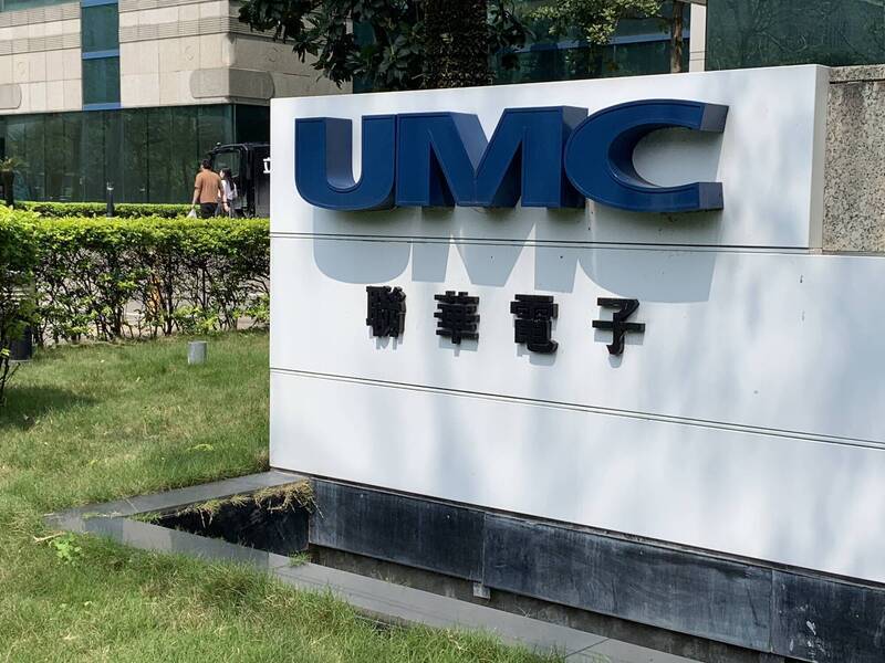
Last Christmas there are many Taiwanese news said UMC will do 12nm technology transfer to Intel and get over 10 billions NTD (>300 millions US dollars) from different stages. The reason of this collaboration is because UMC's 12nm process is for ARM structure which is complementary to Intel's nodes that are focused on the x86 structure.
Last Christmas there are many Taiwanese news said UMC will do 12nm technology transfer to Intel and get over 10 billions NTD (>300 millions US dollars) from different stages. The reason of this collaboration is because UMC's 12nm process is for ARM structure which is complementary to Intel's nodes that are focused on the x86 structure.
That is an interesting thought. Gang up against TSMC. The IBM alliance failed because IBM semiconductor failed at 28nm HVM and was given away. Intel has a much better chance at this since they would be the unquestioned leader of the gang. UMC, Tower, maybe GF? GF has 14/12nm but nothing after that. Samsung? That would be interesting. How well would Samsung and Intel get along? They have to do something because TSMC is running away with it. TSMC N2 is gaining momentum fast. I still have not found an Intel 18A or Samsung 3nm design start. Lots of people are looking at the PDKs but no big chip design starts.
UMC Building effectively a brand new FAB in Singapore to at least double the output of the FAB12i here.
It look almost complete , will have a look tomorrow and take some pictures if the weather is nice!
Seems like a win/win. Intel gets increased ROIC/ROA on fully depreciated fabs that they don't have much use for. UMC gets a low-capital approach to serving their customers on a new node, that adds geographic diversity. Both share the costs of a node and foundry ecosystem ramp-up that already has a pool of prospects via the UMC customer base.
Seems like a win/win. Intel gets increased ROIC/ROA on fully depreciated fabs that they don't have much use for. UMC gets a low-capital approach to serving their customers on a new node, that adds geographic diversity. Both share the costs of a node and foundry ecosystem ramp-up that already has a pool of prospects via the UMC customer base.
I was told that the 12nm process in question will be TSMC compatible? UMC 14nm was not and why would TSMC allow this? This is very strange but would explain why it is being done.
All of UMC's CMOS processes are TSMC compatible. They use the same design rules. SMIC, UMC, Chartered (now GF) all used TSMC compatible PDKs through 28nm. This allowed customers to take their GDSII to multiple foundries for 2nd and 3rd source manufacturing. I remember one QCOM design that was at four foundries. They did this to get the best pricing. It was not possible at FinFETs so it stopped at 28nm. At least I did not think it was possible.
All of UMC's CMOS processes are TSMC compatible. They use the same design rules. SMIC, UMC, Chartered (now GF) all used TSMC compatible PDKs through 28nm. This allowed customers to take their GDSII to multiple foundries for 2nd and 3rd source manufacturing. I remember one QCOM design that was at four foundries. They did this to get the best pricing. It was not possible at FinFETs so it stopped at 28nm. At least I did not think it was possible.
Smart move, just like renting out to Tower. The IFS bottleneck is as much management and knowing your customers, as it is building fabs. Arguably Intel reliably has the talent to build and operate. So this is in some ways a step beyond foundry business model, it is more like retail has become with an overall facility like a mall hosting many boutiques with a shared infrastructure but different market segments.
If UMC and Intel cooperate to adjust the process Intel will run to support the process that UMC has, it makes sense. Presumably Intel agrees to tweak some machines and UMC agrees to provide the knowledge and recipes.
Here is the official word from Pat on the investor call:
We are also very pleased to have completed a major agreement with United Microelectronics, or UMC, to develop a 12-nanometer process platform targeting high-growth markets, including mobile, communication infrastructure and networking. This expands both Intel and UMC's foundry process portfolios and customer access to a broader and more resilient supply leveraging our Arizona site.
This agreement builds upon and furthers our long and deep relationships with the vibrant Taiwan ecosystem. This also meaningfully extends the production life of our installed capacity and improves our returns on investments, similar to the announcement last quarter of our Tower Semiconductor partnership at the 65-nanometer node with our New Mexico site.
I'd also add things like we just announced with UMC, right. We're taking older factories. And as Tim, as you might've heard me say in the past right, a bug in the Intel business model, right. Just when a factory got very good and depreciated, we moved to the next node.
Pat Gelsinger
"Our success with IFS will be measured by customer commitments and revenue. We have taped out more than 75 ecosystem and customer test chips. IFS already has more than 50 test chips in the pipeline across 2024 and 2025, 75% of which are on Intel 18A."
The 18A PDK is v .9 with 1.0 being the official production version so it is getting close to design start time.
Pat Gelsinger
We have taped out more than 75 ecosystem and customer test chips. IFS already has more than 50 test chips in the pipeline across 2024 and 2025,
If only comparing to the tapeout number tsmc talked about in his earnings call (typically 60~100 in 2 years), 2 years 75 customer test chips tapeout seems normal. But the tricky part is what does it mean of customer test chips? Real product or just some test chips for design rule check, SPICE, IP test/qualification....