Design process retargeting is a common recurrence based on scaling orBOM(Bill-Of-Material) cost improvement needs. This occursnot only with the availability of foundry process refresh to a more advanced node,but also to any new derivative process node tailored towards matching design complexity, power profile or reliability needs. While many design companies rely on foundry supplied baseline DRC (Design Rule Checks) and LVS (Layout Versus Schematic) rule decks that correspond to each process roll-out, the shift to new technology such as FD-SOI(Fully Depleted Silicon On Insulator) and FinFET injected more complex design verification needs.
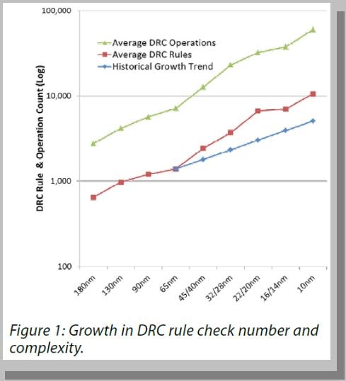
During the past five years, the continuous process migration prompted DRC rules explosion in term of complexity and quantities such as due to multi-patterning, voltage-aware DRC, or FinFET specific requirements (e.g. cell alignment, polygon shift). Figure 1 shows the trend. Hence, the traditional DRC rule based verification which involved running foundry rule-sets is no longer adequate. Instead, a robust reliability verificationenvironment is necessary to ensure a successful tape-out. In fact, foundry selection is increasingly hinged upon its availability.

Intellectual Property (IP) reuse is an integral part of a design refresh and is taking a significant portion of design remapping efforts in addressing these aspects:
- IP porting needs (physical footprint, power target, etc.)
- IP validation in new context and across different IP’s.
- If process scaling involved, handling special IP design aspects such as the Electro-Static Discharge (ESD) requirement for IO pin protection and its adjoining interconnect.
- Validation of IP interaction at full-chip context to further complement stand-alone block level checks, which includes performing its reliability verification.
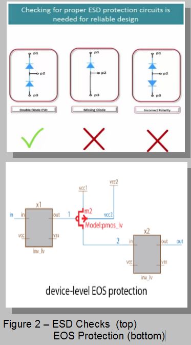
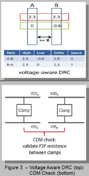
There are a few key aspects covered in reliability verification as illustrated in Figures 2 and 3:
- Design level ESD–ESD is widely known and normally causes irreversible circuit damage. Several protection schemes to mitigate this includes common double-diode ESD network. Mentor’s Calibre PERC high-level checks GUI enables the description of these protection circuits in the form of a Calibre rule-check with minimum effort.

- Device levelElectrical Over Stress (EOS)–EOS could be described as a thermal induced damage due to over-voltage or over-current application to a device.In low-power applications, the presence of high-voltage signals and the use of thin oxides introduce vulnerability of layout to electrical overstress and may lead to oxide breakdown. In multi-voltage domain design, depending on how nets traverse within a design, signals of different voltages may be near each other. This difference in voltage values can create electrical fields that can influence sensitive areas on the chip and lead to reliability issues, particularly for automotive and other high power applications. To protect these nets from Time-Dependent Dielectric Breakdown (TDDB), usually caused by having nets too close to each other for their respective voltages, additional spacing rules are developed that specify power domain spacing based on the voltage delta.Calibre PERCtool voltage propagation feature enables designers to perform automated static analysis on large designs efficiently.
- Voltage Aware DRC –Once netlist is extracted from the layout, Calibre PERC traces voltages throughout a design without the use of SPICE simulations or manual markers. It identifies nets and devices subject to voltage-aware DRC constraints, pinpoint nets voltages of interest and its gradient with relevant net counterparts then used them to run DRC net spacing checks. These checks not only enable robust protection against TDDB, but also enable design teams to save significant design space by applying only the spacing required for each voltage combination.
- Interconnect Robustness Checks – Interconnect linking IP to the ESD protection circuitries at device level by using Point-to-Point (P2P) or assessing Current Density (CD) violation to complement chip-level validation. Charge Device Model (CDM) checking is crucial on gates that are directly connected to power/ground due to shrinking gate-oxide thickness.

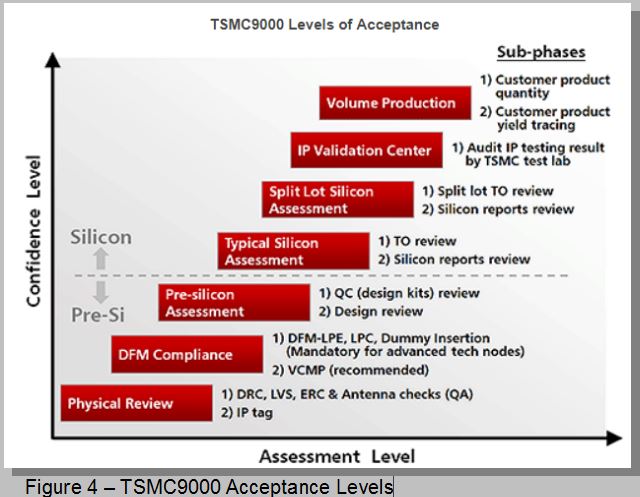
Most foundries nowadays have provided baseline reliability rule decks and leveraging Calibre PERC reliability platform. TSMC rolled-out TSMC9000IP for both library and IP quality management program. On supported nodes all TSMC IP’s with 100% score have been validated by Mentor’s Calibre PERC. Moreover, itwas selected as the EDA reliability platform by the RESCAR2.0 program. It is driven by a consortium of six major car and supplier companies (Audi, BMW, etc.) and the German government. Their aim is to enhance the reliability and robustness electronic automotive components, which reflects conformance to the international functional safety standard ISO 26262. The collaboration has also yielded Calibre automotive reliability checks. Tower Jazz is the first commercial foundry to incorporate them into their standard Calibre PERC design kit offering.
In summary, demanding markets such as automotive and IoT dictate rigorous need of both internal and third-party IP’s validation, which should include reliability verification. A more streamline and robust set of checks is crucial to complement foundry-provided, rule based checks. Mentor’s Calibre PERC platform provides such design kit and accommodates further customization needs to satisfy such demands. For more info on Calibre, please check Mentor’s white paper here.


Comments
There are no comments yet.
You must register or log in to view/post comments.