At the SPIE Advanced Lithography Conference held in February, ASML presented the latest information on their Deep Ultraviolet (DUV) and Extreme Ultraviolet (EUV) exposure systems. I recently got to interview Mike Lercel of ASML to discuss the presentations.
DUV
Despite all the attention EUV is getting, most layers are still exposed with DUV systems and this will likely continue to be true for the foreseeable future.
ASML has had two DUV platforms in production, the XT platform for dry exposure tools and the NXT platform for immersion. The NXT is the faster and more sophisticated platform.
For leading edge immersion, ASML has introduced the NXT:2050i on the fourth generation NXT platform for ArF immersion (ArFi). The new system has a new wafer handler, wafer stage, reticle stage, projection lens, laser pulse stretcher and immersion hood. This results in faster wafer to wafer sequencing, faster measurements, pellicle deflection correction and improved speckle with improved overlay. Throughput on the new system is 295 wafers per hour (wph). Longer term there are plans for a 330 wph system (see figure 1).
ASML is now taking the NXT platform and porting dry lenses onto it with the first system the NXT:1470 for ArF dry offering 300wph (slightly faster than the NXT:20250i because it does not have the immersion overhead). The 300 wph for the NXT:1470 is up from approximately 200 wph for the XT:1460K. In the future the NXT:1470 will have further throughput improvements to 330 wph (see figure 1).
There are also plans to port a KrF dry lens to the NXT platform with 330 wph planned (see figure 1).
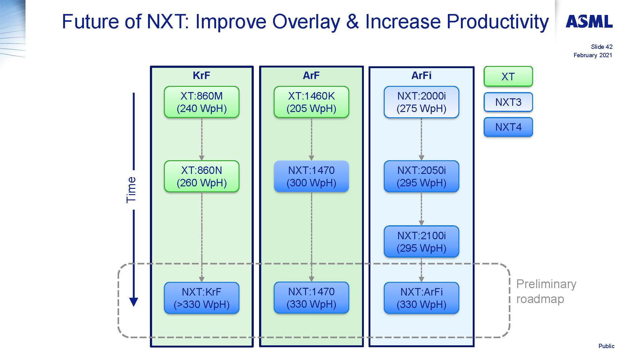
Figure 1. NXT Roadmap.
EUV (0.33NA)
With the standard 0.33 numerical aperture (NA) systems in use at Samsung and TSMC for 7nm and 5nm logic production and at Samsung for 1z DRAM, the number of wafers exposed with EUV is growing rapidly (see figure 2).
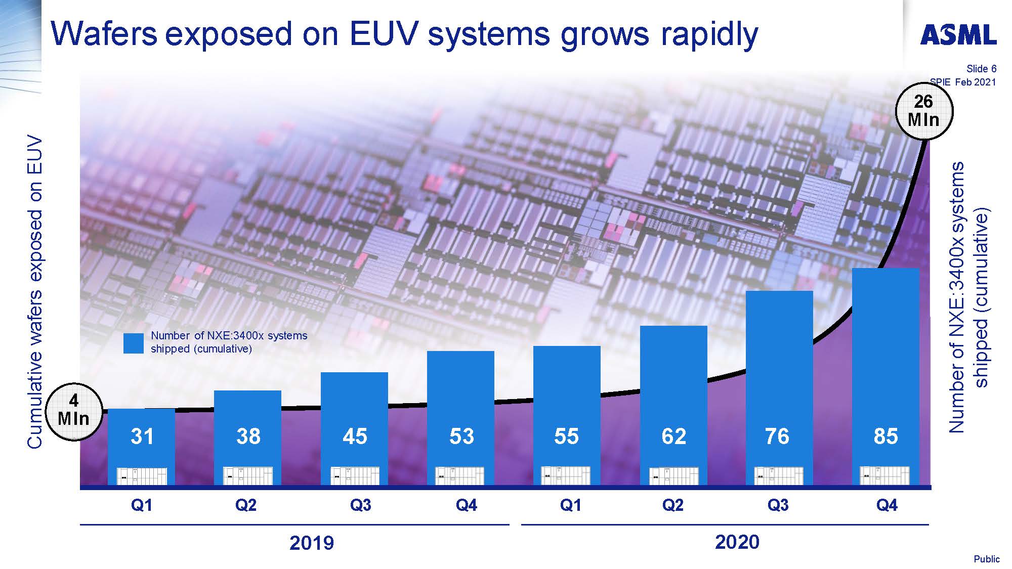
Figure 2. 3400x EUV Systems in the Field and Wafers Exposed.
The NXE:3400C system has been shipping since late 2019 and the new NXE:3600D should start shipping later this year. Each new system provides improved throughput and overlay.
Figure 3 presents a summary of both 0.33 NA and High-NA 0.55NA systems to be discussed in the next section.
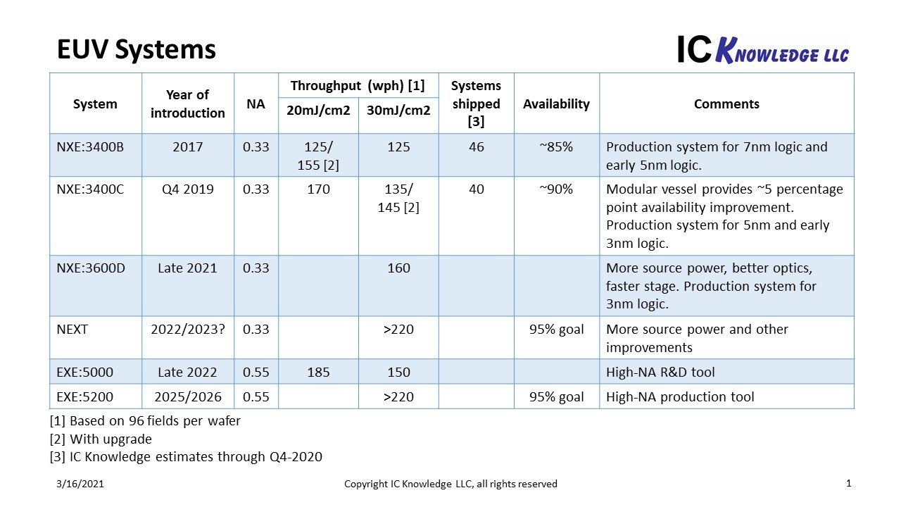
Figure 3. EUV Systems Summary.
- The first column lists past, current, and future systems beginning with the NXE3400B systems that were the first production systems.
- The second column provides the introduction dates for each system. Notably the new NXE:3600D should ship later this year with improved performance and the first high-NA systems should ship late 2022.
- The third column presents the numerical aperture of the system with 0.33NA representing the current system and 0.55NA the high-NA system in development.
- The next two columns present the throughput for 20mJ/cm2 and 30mJ/cm2 doses as demonstrated by ASML. These throughputs are based on 96 fields per wafer more typical of a DRAM application.
- The systems shipped is IC Knowledge’s estimate of the number of NXE:3400B and NXE:3400C systems shipped by type through Q4-2020, ASML does not provide this breakout.
- The next column is the current availability of approximately 85% for the NXE:3400B and approximately 90% for the NXE:3400C. The 3400C has the new modular vessel that reduces downtime. Long term ASML has a goal to reach the 95% availability typical of DUV systems.
- The final column presents some comments on the systems and usage. We believe that 7nm logic production has primarily been on the 3400B and 5nm on the 3400C. We expect the 3nm processes due to enter production over the next one to two years to be primarily produced on the 3600D systems.
A key enabler for EUV of dense patterns is the availability of a pellicle, there is now a usable pellicle available. Pellicles use reduces throughput and whether a pellicle is used or not depends on the pattern density being printed. Figure 4 presents the state of EUV pellicle transmission.
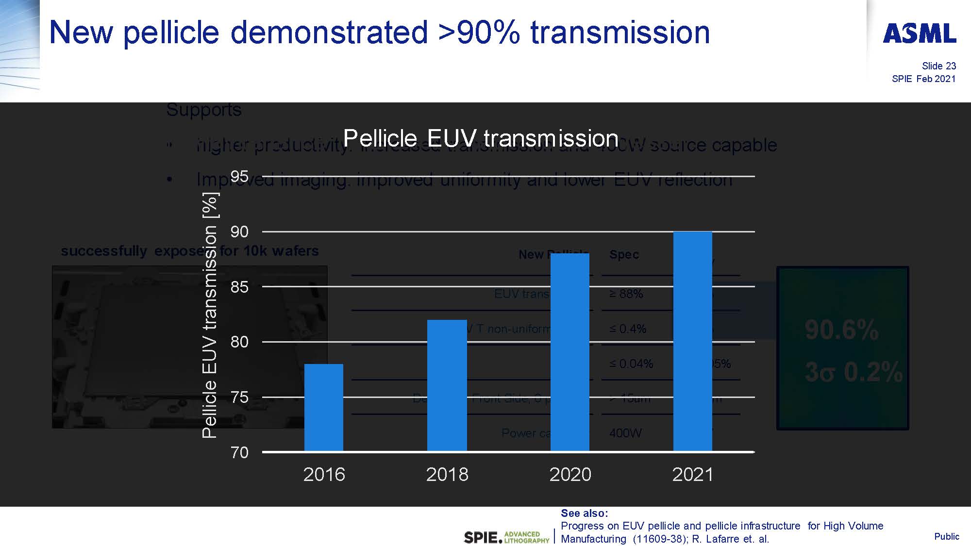
Figure 4. EUV Pellicle Transmission.
There is currently some pellicle use in production.
High-NA EUV (0.55NA)
High-NA has now progressed from PowerPoint slides through engineering design to building modules and frames. The first High-NA tools (0.55NA) are expected to ship in late 2022. These EXE:5000 systems will likely be used for research and development with the EXE:5200 systems due in 2025/2026 being the first high-NA production systems (see figure 3).
The current 0.33NA systems can print down to an approximately 30nm pitch with a single exposure. There is work being done now to demonstrate 28nm and eventually 26nm lines and spaces with a single exposure. TSMC’s 5nm process currently in production has a 28nm M0 pitch and we believe this one layer may be double patterned EUV in current production while the rest of the layers that use EUV are single patterned. For TSMC’s 3nm process due to begin risk starts later this year we expect several EUV double patterned metal layers. With the current timing for 0.55NA systems to enter production estimated to be in the 2025/2026 time-frame, we may see foundry 2nm and Intel 5nm processes in production before then with extensive EUV double pattering. 055NA EUV would likely first appear in production for foundry 1.5nm processes and Intel 3nm eliminating EUV double patterning and reducing costs.
Figure 5 presents the technical value of High-NA EUV.
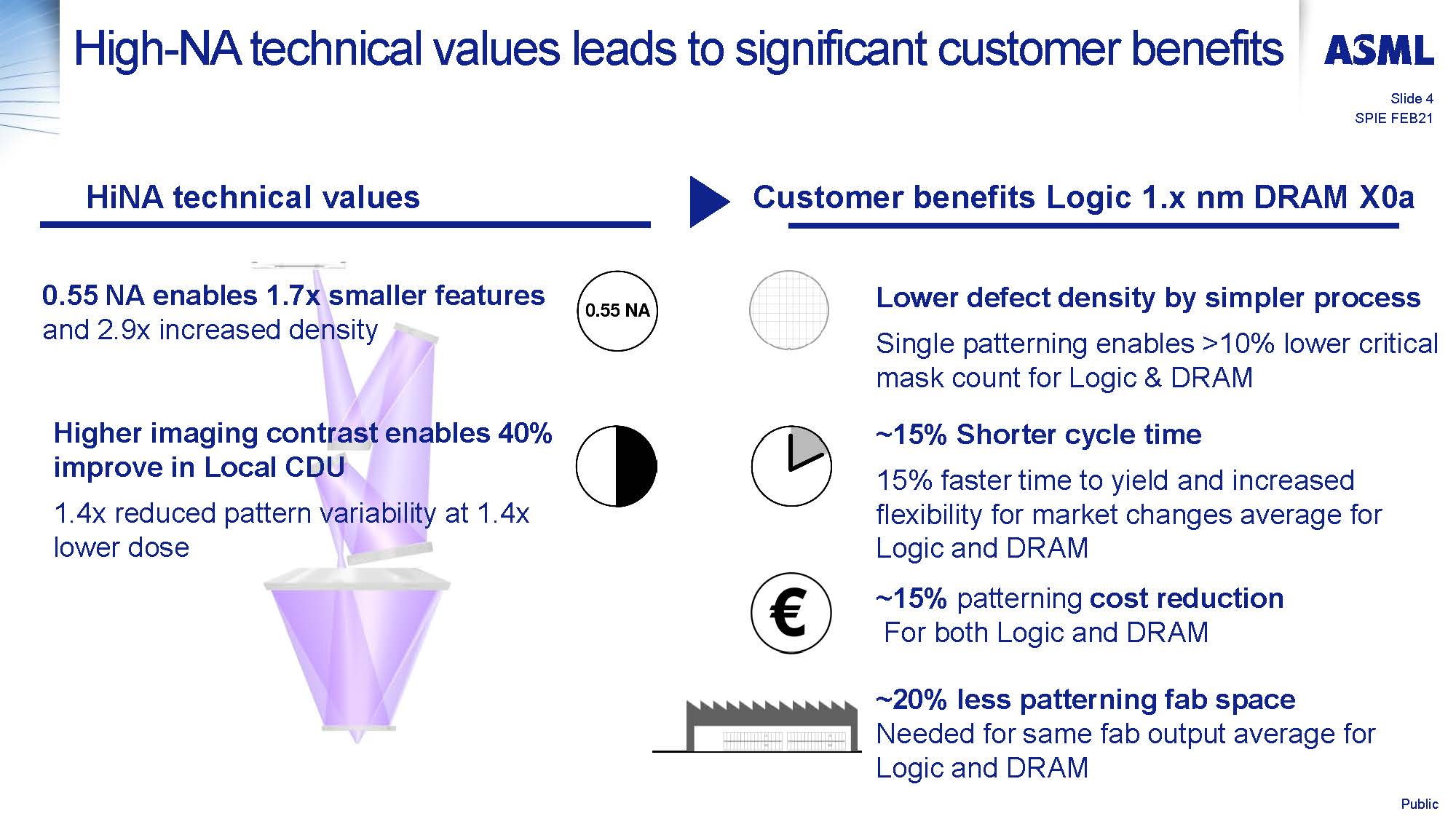
Figure 5. High-NA Technical Values.
One other value to 0.55NA EUV is that the higher contrast can print dense features with a much lower dose than 0.33NA EUV improving throughput (figure 3 is throughput for specific doses and does not consider dose reduction). Figure 6 illustrates the 0.55NA advantage.
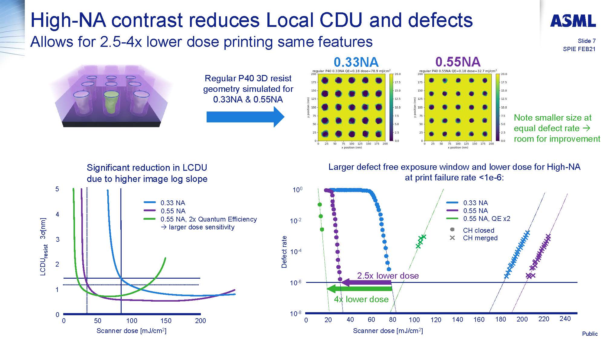
Figure 6. High-NA Throughput Advantage for Dense Patterns.
There is also work being done on improved EUV mask absorber layers to improve contrast and resolution, see figure 7. and improve photoresists, see figure 8.
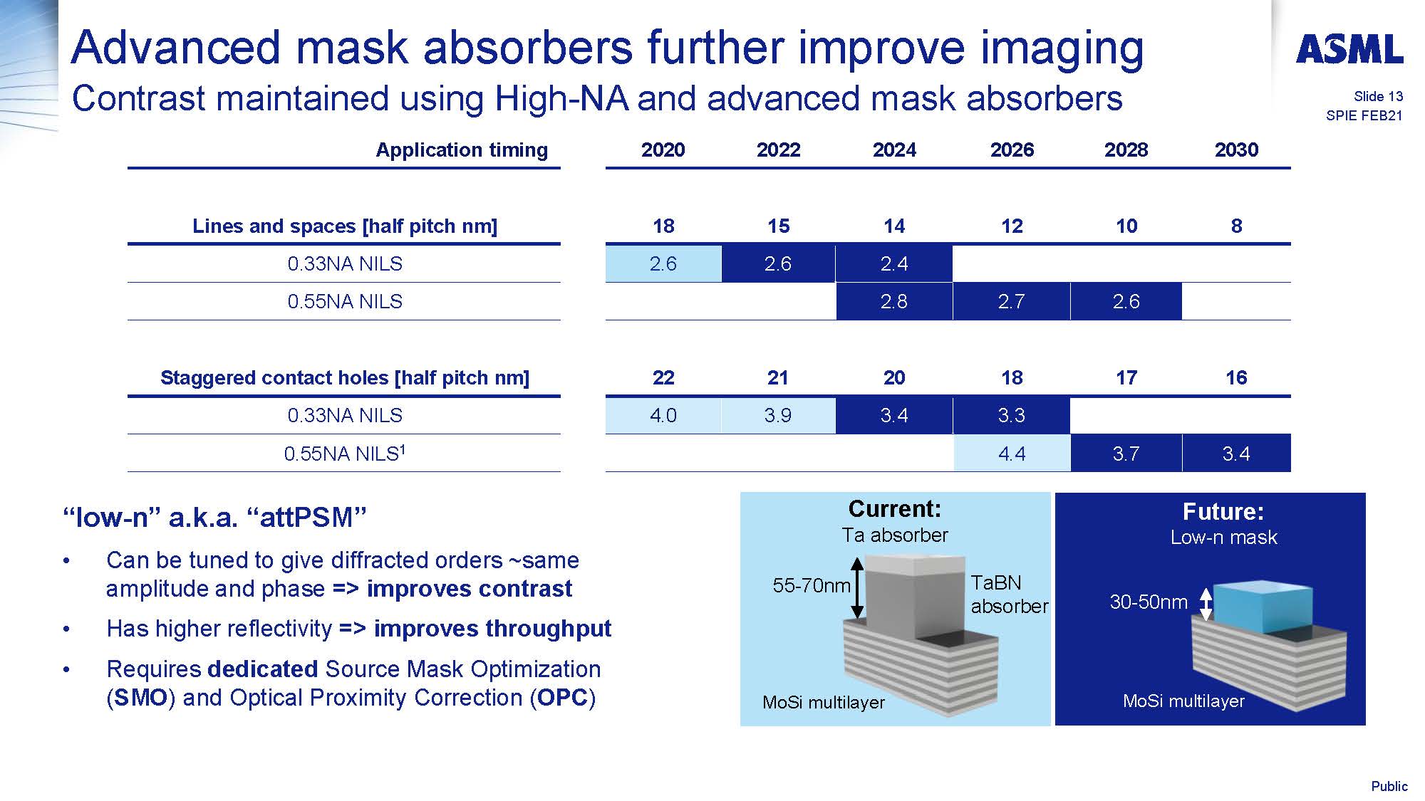
Figure 7. Improved Mask Absorber Layers.
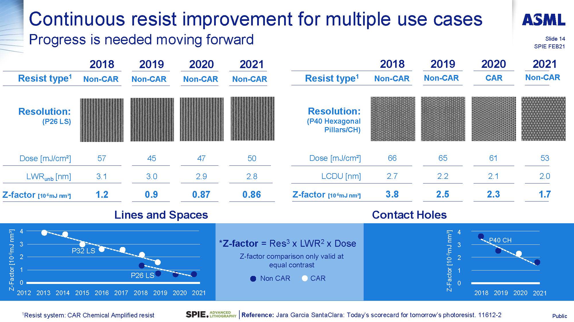
Figure 8. Improved Photoresist.
Currently modules and frames for high-NA tools are being fabricated.
Conclusion
ASML continues to drive throughput and resolution across their entire portfolio of DUV and EUV systems. With High-NA system manufacturing underway, a path to 1.5nm logic and beyond is underway.
Share this post via:


Musk’s Orbital Compute Vision: TERAFAB and the End of the Terrestrial Data Center