
- This event has passed.
SPIE Advanced Lithography + Patterning
February 25 - February 29
Share your research, challenges, and breakthroughs with colleagues in San Jose
The call for papers is open. Submit your abstract and join other leading researchers who are solving challenges in optical and EUV lithography, patterning technologies, metrology, and process integration for semiconductor manufacturing and adjacent applications.
Conferences and courses: 25 – 29 February 2024
Exhibition: 27 – 28 February 2024
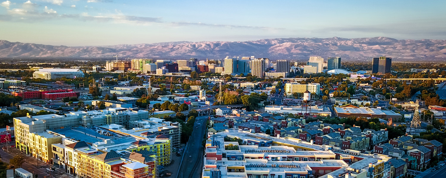
As a center of innovation, San Jose welcomes you
San Jose, California in the U.S. boasts the largest concentration of technology expertise in the world. San Jose also leads the nation in patent generation. The city has 25 companies with 1,000 employees or more, including the headquarters of Adobe Systems, BEA Systems, Cisco, Xilinx, Lam Research, and eBay, as well as major facilities for Flextronics, Hewlett-Packard, IBM, Hitachi, Agilent Technologies, and Lockheed Martin.
Plan to join other leaders eager to learn about emerging technology
Enrich your work by attending the most important conference for optical and EUV lithography, patterning technologies, metrology, and process integration for semiconductor manufacturing and adjacent applications.


Real men have fabs!