





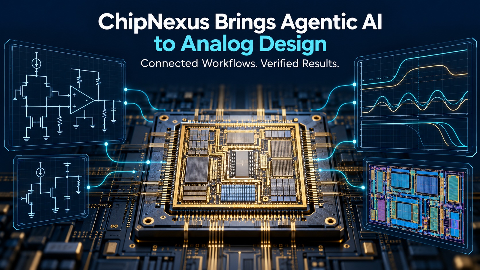
ChipNexus has introduced its NEX Analog Agent, bringing conversational automation to analog engineering workflows built around Cadence Virtuoso, Spectre simulation and Siemens Calibre physical verification. Available now, the software operates with customers’ installed tools, licenses and process design kits, giving teams a way to adopt agentic AI within familiar development environments.
The announcement targets a demanding part of semiconductor development. Analog and mixed-signal engineers must repeatedly connect circuit intent with electrical behavior, layout constraints and verification results. NEX aims to carry more of that execution through a single conversation while keeping reported outcomes tied to evidence from the underlying tools.
Connecting the Engineering Workflow
The Analog Agent coordinates project setup, schematic work, layout, simulation, physical verification and reporting. It delegates stages to specialized Virtuoso sub-agents with defined tools and acceptance criteria.
Engineers can ask the platform to inspect libraries, device parameters and symbol pins; read or modify schematics and layouts; export netlists; execute Spectre simulations; and interpret results. It can also run Calibre design rule checking and layout-versus-schematic verification, exchange GDS layout data and compare layouts with a reference.
A representative workflow starts with inspecting a circuit, making a bounded schematic change and measuring its effect through simulation before proceeding to layout. Connecting those steps could reduce the repetitive coordination engineers otherwise perform between individual applications.
The value comes from maintaining continuity: carrying the objective, design context and acceptance criteria through successive operations.
Showing What Actually Passed
ChipNexus emphasizes a distinction that matters for engineering automation: successfully running a tool does not necessarily mean successfully completing a task.
Its stage reports separate work that passed, work that executed but missed acceptance criteria, and work that could not run. A design rule check containing violations or a layout-versus-schematic mismatch remains incomplete and returns for repair.
The agent also checks device operating points and presents performance alongside process corner, temperature, supply and load conditions. Those details are essential because a circuit measurement means little without knowing the circumstances under which it was obtained.
This reporting approach could make AI-assisted work easier to review. Engineers receive a record of verified outcomes and unresolved issues, providing a firmer basis for deciding what should happen next.
Remembering Verified Fixes
Another practical feature is persistent error memory. When the platform resolves a recurring environment problem, it records the verified fix for reuse in later sessions within the same repository, including across Git worktrees.
Examples include required module loads, tool-specific command flags and shell behavior. These may appear minor, but repeated setup failures can interrupt otherwise productive automation.
Engineers can inspect, update or disable memory entries. That control helps keep accumulated operational knowledge useful as environments and project requirements change.
Early Customer Experience
ChipNexus reports that analog and RF engineers at an unnamed semiconductor customer used the agent for device characterization across five topologies. Tasks included netlist generation, simulation setup, frequency sweeps and plotting.
According to the announcement, an RF engineer validated designs operating above 10 GHz across three process technologies, with agent-supported setup, sweeps and analysis taking one to two hours per process node.
The example offers a concrete indication of workflow scope. Without a published comparison against the customer’s previous process, however, it does not establish a quantified productivity improvement.
Analog design combines scarce expertise with extensive iteration. Automating execution around trusted tools could let engineers spend more time evaluating circuit behavior and less time managing commands, environments and handoffs.
NEX’s use of existing licenses and PDKs also lowers the disruption associated with adoption. Private-cloud and on-premises deployment options give organizations flexibility over where the platform operates.
Bottom Line: The broader significance is an engineering model in which agents execute connected tasks, preserve useful knowledge and expose evidence for human review. It expands analog teams’ capacity to explore alternatives while maintaining control over design decisions, verification and final acceptance, absolutely.
Also Read:
CTO Interview with Taylor Barton of Certus Semiconductor
NIST Sets a Clearer Course for the Post-Quantum Security Transition
CTO Interview with Ed Plowman of Imagination Technologies
Share this post via:


The $725 Million Chip Development: Why Execution Risk, Not IP Cost, Now Dictates Advanced-Node Survival