A new term has entered the vernacular of electronic design engineering — pathfinding. The complexity of the functionality to be integrated and the myriad of chip, package, and board technologies available make the implementation decision a daunting task. Pathfinding refers to the method by which the design space of technology options is reduced to a viable solution, evaluating system parameters and goals against different technical alternatives. The increasing momentum in (2.5D/3D) packaging technology has added significantly to the choices available for implementing and interconnecting the functional design, making path finding a prerequisite to implementation.
Pathfinding is much more intricate than simply partitioning functions between chips. Partitioning algorithms generally seek to minimize some objective by clustering system functions with “high affinity” together into distinct subsets for physical implementation. Conversely, path finding requires exploring the impact of implementation decisions across disparate physical domains — it encompasses a much larger space of chip/package/board design considerations:
- chip macro floorplan, redistribution layer (RDL) routing, and I/O bump patterns
- optimal package fan-out trace patterns
- interposer (or TSV) via and RDL design, for multichip packaging options
- board routing complexity
All these options have a direct bearing on product cost, to be sure. These implementation decisions much also ultimately satisfy signal integrity, power integrity, and thermal reliability requirements, as well.
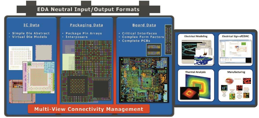
A major concern in enabling engineering teams to pathfinding is that the physical and electrical data for chip, package, and board reside in different data formats and unique representations. Making implementation decisions across these design domains requires a single, consistent view — resulting project edits and revisions require appropriate communication of ECO’s back to the original databases.
At the recent DesignCon 2016, I had an opportunity to meet John Park, Methodology Architect at Mentor Graphics, and learned how Mentor has addressed these difficult pathfinding issues in their recently announced Xpedition Package Integrator product. John emphasized that their approach was architected to utilize design data coming from various sources, and that the development team provided the interfaces necessary to incorporate the requisite information into Package Integrator.
In John’s words: “The approach we followed had to be EDA neutral.”
All system connectivity is maintained within Package Integrator, while designers are pursuing their path finding optimizations, as highlighted in the figure below.
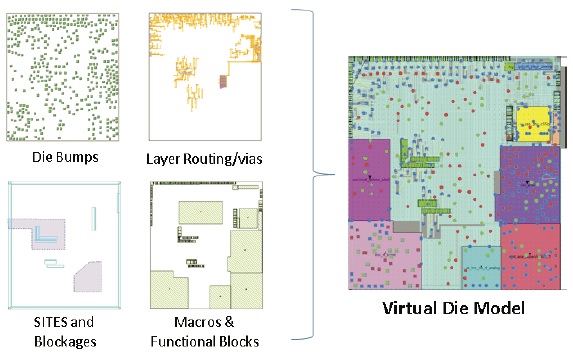
A key design data interface into Package Integrator provides a Virtual Die Model, an abstract of the detailed chip layout data suitable for pathfinding. For existing die, a simple abstract of area + pad array + pin name data will suffice. Yet, initial pathfinding will involve chip designs that are still fluid. In these cases, the Virtual Die Model includes the additional data necessary to evaluate chip-interposer-package implementation decisions. As illustrated in the figure below, chip floor plan data — e.g., macro placements, blockages — are required with the die bump pattern. Edits to the floor plan, chip RDL, bumps, and/or package traces are enabled in Package Integrator, to provide visual feedback as to routing congestion (and thus, cost).
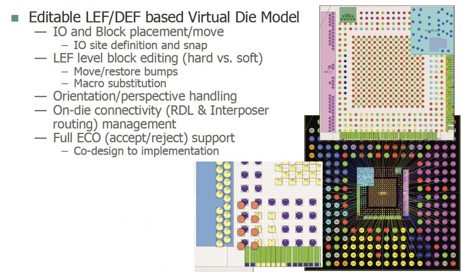
The figure below illustrates a specific example of using the Virtual Die Model to evaluate die and package implementation data in a single view. A die floor plan macro (in light blue) is depicted, with the corresponding bump pattern-to-BGA package ball placement and trace connectivity. Edits to the macro LEF placement are enabled, with any resulting proposed ECO’s maintained by the project management supervisor functionality within Package Integrator. These ECO’s can then be reviewed, approved and forwarded, or rejected.
These pathfinding edits must be rule-driven, to ensure a design requirement is not violated. For an example of a user-defined rule, John described the definition of a specific (+ve, -ve, IOVDD, GND) bump array configuration to be used for a differential signal — any edits to bump locations are verified to be consistent with the rules database. John also briefly highlighted examples of the pathfinding activity and rules checking associated with die-to-interposer via and bump assignment, as well.
A path finding solution requires a view of all domains, as illustrated in the die/package/board example below.
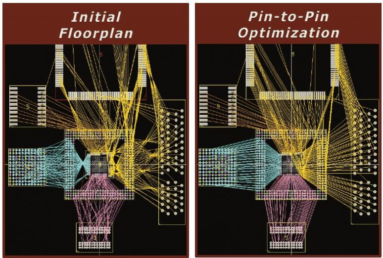
The connectivity flightlines between die, packages, and board-level connectors illustrate how congestion can be alleviated by path finding decisions on pin assignment and placement. Specific pin-to-pin routes can be applied. If routed traces are available, an interface to EM model generation and signal integrity analysis is also provided in Package Integrator. Utilizing thermal models for the individual die, a computational fluid dynamics (CFD) thermal analysis of the full system is enabled, as well.
The optimization of a product implementation across the physical boundaries of each die, (2.5D/3D) packages, and board requires a single view of the design data, with a corresponding connectivity model. This view must be agnostic to the source of the data, and must provide ECO project management. This complex co-design activity, aka pathfinding, must also support appropriate rules and constraints, verifying proposed edits within each domain.
Mentor Graphics has recently announced Xpedition Package Integrator to assist product architects and designers with the pathfinding task. They focused on developing data interfaces and model abstracts to be independent of the EDA source. They have successfully bridged the gap between the different physical domains, to enable key (and early) implementation optimizations.
-chipguy
Share this post via:


Comments
0 Replies to “Pathfinding to an Optimal Chip/Package/Board Implementation”
You must register or log in to view/post comments.