You are currently viewing SemiWiki as a guest which gives you limited access to the site. To view blog comments and experience other SemiWiki features you must be a registered member. Registration is fast, simple, and absolutely free so please,
join our community today!
A new term has entered the vernacular of electronic design engineering — pathfinding. The complexity of the functionality to be integrated and the myriad of chip, package, and board technologies available make the implementation decision a daunting task. Pathfinding refers to the method by which the design space of technology… Read More
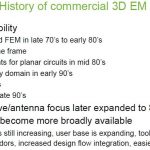
Expanding 3D EM Simulation Access to Allby Tom Dillinger on 02-03-2016 at 7:00 amCategories: Cadence, EDA
James Clerk Maxwell’s eponymous equations are the basis for simulating electromagnetic wave propagation. In school, EE majors tended to fall into two camps: (a) those that thoroughly enjoyed their fields and waves classes, who liked doing surface integrals, and who were adept at demonstrating the “right hand rule”, and (b) … Read More
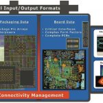
DesignCon is a unique conference — its tagline is “Where the Chip meets the Board”. Held each January in Santa Clara, the conference showcases a wealth of new technologies for advanced packaging, printed circuit board fabrication, connectors, cables, and related analysis equipment (e.g, BERT, VNA, scopes). Of specific… Read More