You are currently viewing SemiWiki as a guest which gives you limited access to the site. To view blog comments and experience other SemiWiki features you must be a registered member. Registration is fast, simple, and absolutely free so please,
join our community today!
I had the opportunity to preview the upcoming SemiWiki webinar titled: Design Methodologies for Next-Generation Heterogeneously Integrated 2.5/3D-IC Designs. John Park’s message, describing this powerful Cadence solution, really impressed me. That’s why I want to encourage you to register for it and join this SemiWiki … Read More
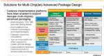
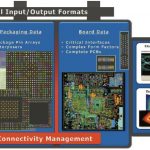
Regular Semiwiki readers are aware of the rapid emergence of various (multi-die) advanced package technologies, such as: FOWLP (e.g., Amkor’s SWIFT, TSMC’s InFO); 2D die placement on a rigid substrate (e.g., TSMC’s CoWoS); and, 2.5D “stacked die” with vertical vias (e.g., any of the High Bandwidth Memory,… Read More
This year is shaping up to be an inflection point, when multi-die packaging technology will experience tremendous market growth. Advanced 2.5D/3D package offerings have been available for several years, utilizing a variety of technologies to serve as the package substrate, interposer material for embedding die micro-bump… Read More
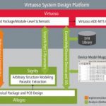
A new term has entered the vernacular of electronic design engineering — pathfinding. The complexity of the functionality to be integrated and the myriad of chip, package, and board technologies available make the implementation decision a daunting task. Pathfinding refers to the method by which the design space of technology… Read More