You are currently viewing SemiWiki as a guest which gives you limited access to the site. To view blog comments and experience other SemiWiki features you must be a registered member. Registration is fast, simple, and absolutely free so please,
join our community today!
The semiconductor industry is experiencing unprecedented growth in complexity as advanced process nodes, heterogeneous integration, and AI-driven workloads demand increasingly sophisticated chip designs. At the same time, semiconductor companies face rising design costs, increasing engineering workloads, and a shrinking… Read More
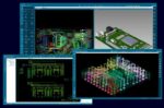
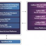
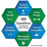
Electronic systems design is filled with a wide range of tools used across IC packaging design, multi-board systems, design creation, physical implementation, electro-mechanical co-design, simulation & analysis, and new product introduction. Siemens has been offering tools in this flow for many years now, so I was able… Read More
Next generation electronic systems require an engineering approach incorporating a digital twin methodology for early verification with digital prototypes. Over the course of a design project, the digital twin model evolves to allow more complex interactions including analysis, simulations and validations earlier… Read More
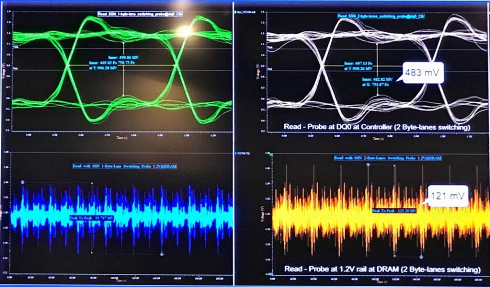
High-speed design requires addressing signal integrity (SI) and power integrity (PI) challenges. Power integrity has a frequency component. The Power Distribution Network (PDN) in designs has 2 different purposes: providing power to the chip, and acting as a power plane reference for transmission-line like propagating … Read More
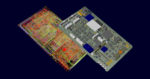
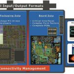
There is an emerging set of advanced packaging technologies that enables unique product designs, with the capability to integrate multiple die, from potentially heterogeneous technologies. These “system-in-package” (SiP) offerings provide architects with the opportunity to optimize product performance, power, cost,… Read More
Consumer electronics demand aggressive mechanical enclosure design — product volume, weight, shape, and connector access are all critical design optimization criteria. Mechanical CAD (MCAD) software platforms are used by product engineers to develop the enclosure definition — the integration of the PCB design… Read More
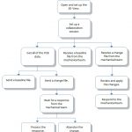
The 4C’s of PCB Designby Tom Dillinger on 04-20-2017 at 12:00 pmCategories: EDA, Siemens EDA
The diamond jewelry industry encourages customers to focus on the 4C’s — cut, clarity, color, and carats. At the recent PCB Forum conducted by Mentor (a Siemens business) in Santa Clara, I learned that current system design flows also require an emphasis on the 4C’s — collaboration, concurrency, consistency… Read More
Anybody who has done any bus & board system design knows the problem. Merchant boards typically have standardized pinouts (after years of haggling in standards organizations) for the backplane bus, and a group of user-defined pins for daughtercard I/O. Homegrown systems usually have a just-as-carefully defined proprietary… Read More
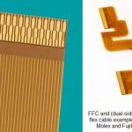
The three F’s of electronic product development are: form, fit, and function. Although the F/F/F assessment typically refers to the selection of the right component, it most definitely also refers to the selection of the proper cabling between assemblies. The requirements for cables are varied, and demanding: ability… Read More
A new term has entered the vernacular of electronic design engineering — pathfinding. The complexity of the functionality to be integrated and the myriad of chip, package, and board technologies available make the implementation decision a daunting task. Pathfinding refers to the method by which the design space of technology… Read More