
3D-IC has a stack of dies connected and packaged together, and therefore needs new testing strategies other than testing a single die. It’s given that a single defective die can render the whole of 3D-IC unusable, so each die in the stack must be completely and perfectly tested before its entry into that stack. Looking at it from a ‘yield’ angle, it’s much better to have a stack of smaller dies (which can have higher yield) than having a large die which can be more prone to defects. So, what should be done to realize that high yield, performance, power and high gate density per unit volume of 3D_IC? Thoughtful orderly sequences of steps have to be performed such that every die work excellent independently and then inside the package together with other dies.

[CoWoS arrangement in TSMC reference flow]
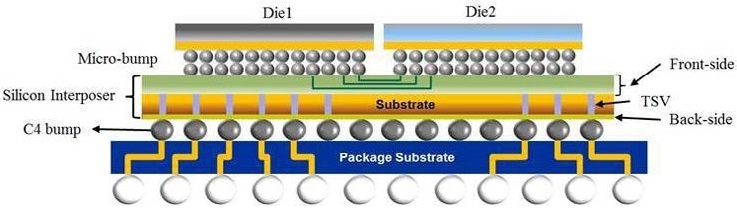
Last year, TSMC’s3D-IC (typically called as CoWoS[SUP]TM[/SUP] – Chip on Wafer on Substrate) reference flow was validated with Mentor’s3D-IC test solution in which an SoC and a Wide I/O DRAM are placed on a passive silicon interposer with about 1200 connections between them. This methodology has been extended further by using TSV (Through Silicon Via) based stacked dies, which requires far less wire length, thus improving performance and interconnection scaling at lesser cost.
Mentor has developed an excellent plug-and-play test infrastructure based on proven standard JTAG (IEEE 1149.1) TAP (Test Access Port) as interface for all dies and IJTAG (IEEE P1687) to model the TAP, test access network, and test components within the die. For accessing the whole package from outside, the TAP at the bottommost die is used, although for testing purpose any die can be used.
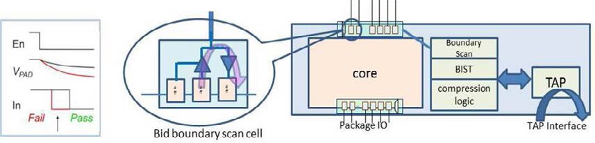
First step is to test each individual die to perfection that includes memory BIST (Built-in-Self-Test) for memories (Mentor provides soft-programmable memory BIST for which algorithms can be applied as needed), embedded compression ATPG with logic BIST for stuck-at, transition, path delay and other timing-aware and cell-aware tests, and die IO test based on boundary scan (IEEE 1149.1). IO wrap test and contactless leakage test are done by using a special test technique called ‘IO wrap’, where bi-directional boundary scan cells are used to set a logic value, tri-state the driver, then capture the input to check that excessive leakage didn’t occur and capture a 0. This boundary scan test technique can be used for thorough die testing, partially packaged device as well as interconnect between packaged dies.
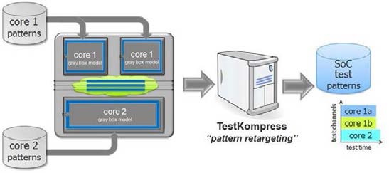
A novel hierarchical DFT methodology provides significant advantages over conventional top-level ATPG. It shortens the design cycle where DFT insertion and ATPG pattern generation can be done at individual block level, thus allowing this activity to start early in the design cycle in more predictable manner. Then the patterns are re-targeted at the top level with appropriate automatic mapping through intelligent software. The patterns for blocks on individual dies are re-used (or merged where required) for complete SoC at the 3D-IC package level. Clearly, smaller test patterns run an order of magnitude faster requiring lesser memory and much efficient scan channel allocation with an order to magnitude fewer tester cycles. Here an important observation must be noted that the DFT logic and ATPG pattern, once created for a die remains valid for the die to be used in any other package as well.
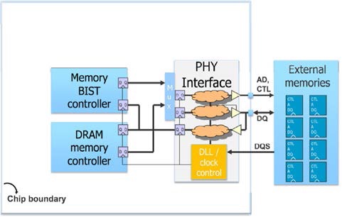
The 3D-IC test methodology allows testing of external memories (usually Wide I/O DRAMs, sourced from different vendors) through JEDEC standard functional pins. Mentor’s special custom interface is used to connect the boundary scan test port to the logic die TAP. With standard interfaces (which may have different internal layouts), the memory die can be swapped when required and new algorithms can be loaded into the soft-programmable memory BIST controller for any targeted testing.
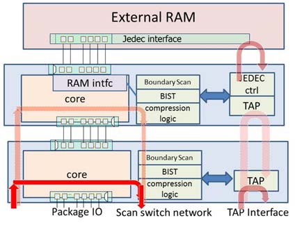
After testing all dies and external memories, interconnects, TSVs and complete package must be tested. The test is managed through the Tap structure on the bottom die which successively enables TAPs on the dies up the chain. IJTAG is used to define the boundary scan network, TAPs, BIST and other DFT logic. Testing is also performed for interconnect between logic and external memory die through JEDEC interface.
To validate the complete assembled 3D-IC, an ordered sequence of tests starting from power-up to interconnections with the Wide I/O memory and at-speed tests are done. A detailed description of this sequence and many other details at each stage is provided in Mentor’s whitepaperauthored by Ron Press, Dr. Martin Keim and Etienne Racine. This plug-and-play test approach based on proven IJTAG standard and existing mature tools provides robustness and flexibility to adapt to any changing requirements.
More Articles by Pawan Fangaria…..
lang: en_US
Share this post via:


Comments
0 Replies to “Smart Strategies for Efficient Testing of 3D-ICs”
You must register or log in to view/post comments.