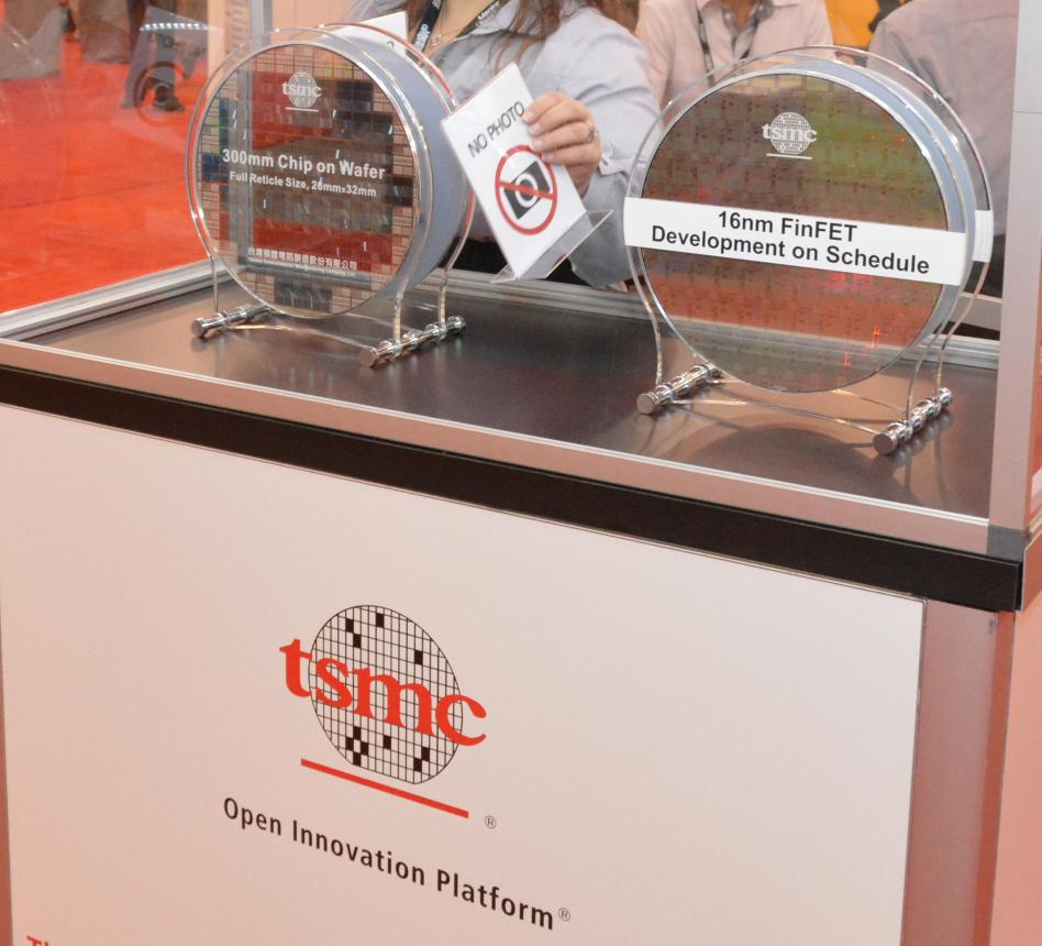
One of the highlights of the TSMC 2013 Open Innovation Platform® Forum was the Partner Award Ceremony. TSMC awarded Berkeley Design Automation (BDA) with the TSMC Open Innovation Platform’s Partner of the Year Award 2013 for joint development of 16nm FinFET design infrastructure. I talked with Ravi Subramanian, BDA CEO, to get his thoughts about the award.
Ravi, BDA has had a long partnership with TSMC, what are the areas have you collaborated in the past?
Dan, as you know we have a long standing collaboration with TSMC driven by our focus on the success of mutual customers. We have collaborated in four main areas: First, the certification of BDA’s Analog FastSPICE (AFS) Platform as part of the TSMC SPICE Qualification Program to 20nm and now on 16nm; Second, the introduction of new circuit analysis technologies in the TSMC Reference Flows, including BDA’s Full-Spectrum Device Noise Analysis and BDA’s Circuit-Specific Process Corners sub-flows. Third, the collaboration to support the validation of TMI and TMI2l and finally, our contribution to the 16nm FinFET design infrastructure including our collaboration to develop the 16nm FinFET SRAM design and characterization flows.
So the work on 16nm FinFET took the partnership to the next level and resulted in this award recognition?
Absolutely. As always, key mutual customers drove the collaboration and BDA was a key contributor to the infrastructure from the very beginning. 16nm is a big shift for the ecosystem, driven by the new FinFET devices which require significant changes in modeling, the complexity of which pushes the limits of circuit simulators.
What areas of the 16nm FinFET design infrastructure did BDA contribute to?
As part of the work on the 16nm FinFET design infrastructure, BDA worked on TMI2 implementation and validation, implementation and validation multiple versions of BSIMCMG device models, qualification of TSMC 16FF successfully through v0.5, and continuing through v1.0, and the support of 4 mutual, leading-edge fabless customers on TSMC 16nm FinFET designs. One major highlight in our contribution is AFS Mega, a breakthrough product BDA introduced earlier this year, which delivers silicon-accurate simulation or memory and other array-based circuits with a capacity of over 100M elements.
What is unique about BDA and the AFS Platform that set you apart from other EDA companies in 16nm FinFET design?
In 16nm FinFET technologies, analog, mixed-signal, and RF design teams face unprecedented and relentlessly increasing challenges driven by high-performance, low-power and high-complexity market demands on the one hand and physical effects such as device noise, layout parasitics, and device mismatch on the other.
In a recent technology forum I participated at CICC last week, it was clear that FinFET will bring big changes to analog and mixed-signal design. BDA is uniquely positioned as the premier platform for nanometer circuit verification supporting all industry flows. With FinFETs come key challenges in device noise analysis, post-layout simulation, digital-dominated-analog design, and variability that stress traditional circuit verification and characterization techniques. BDA’s’ solutions are providing customers the confidence that they can handle these FinFET challenges. Continued R&D investment in new technologies introduced into the AFS Platform, such as ACE (Analog Characterization Environment) and other Silicon Engineering technologies, helps our customers manage the growing complexity of mixed-signal design in the deepest nodes. Our customers’ confidence in our platform is the only real metric we can use to measure our success.
What is the benefit of this collaboration with TSMC for your mutual customers?
Mutual customers get a qualified circuit verification flow at every TSMC process node, enabling reliable and robust design. Customers put their trust and confidence in BDA and TSMC when BDA delivers the simulator accuracy while TSMC delivers device models that have very accurate model parameter extraction and include the required device noise model parameters and statistical behavior to support circuit verification and characterization.
By working together to validate capabilities such as device noise analysis, circuit-specific statistical corners, and 16nm FinFET design infrastructure, BDA and TSMC deliver a flow that has been validated ahead of time, removing the guesswork from our mutual customers.
What’s next for the TSMC BDA partnership going forward?
We are excited to continue to support the development and deployment of FinFET technologies and new verification /characterization methodologies to mutual customers designing analog mixed-signal, and RF ICs. We have also been busy looking at enabling customers using planar technologies in applications such as ultra-low power circuits, sensors/mems solutions, and 28nm RFCMOS flows – areas where nanometer circuit verification is vitally important for our mutual customers.
lang: en_US
Share this post via:


Solving the EDA tool fragmentation crisis