





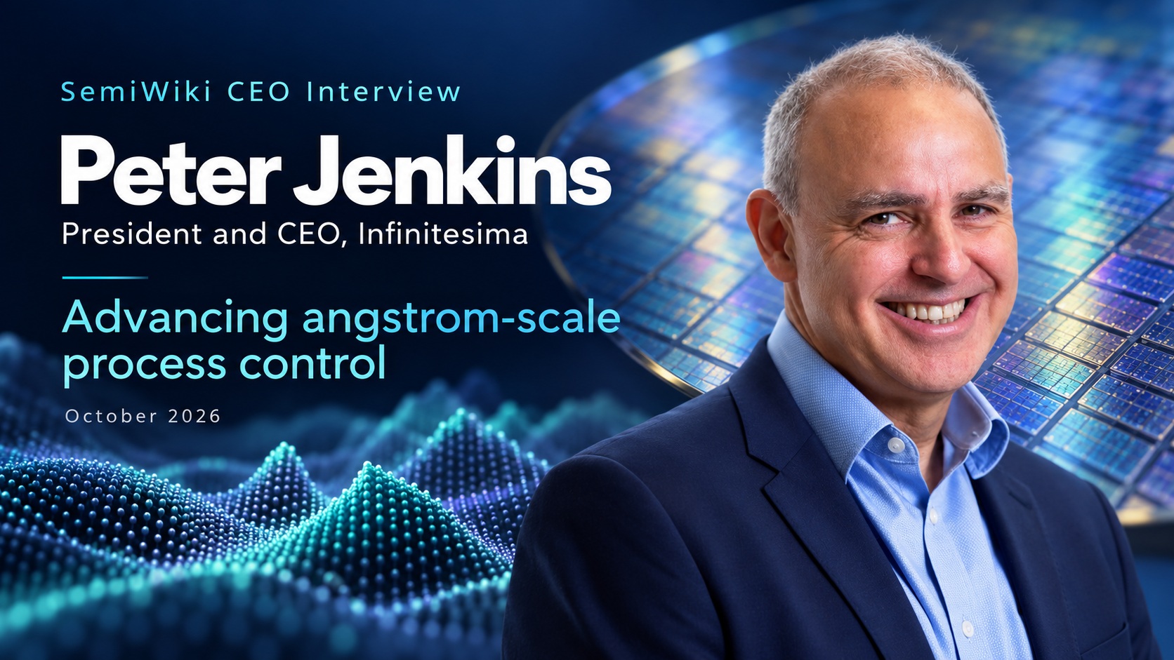
As CEO, Peter Jenkins, leads the development and commercialisation of angstrom-scale process control technology, helping semiconductor manufacturers gain deeper process insights, improve yields and enable the next generation of advanced devices.
His international career has also included roles in the Netherlands, South Korea and Hong Kong and prior to joining Infinitesima, he spent 27 years at ASML, holding senior leadership positions across engineering, manufacturing and operations. This experience provided a deep understanding of the challenges involved in bringing breakthrough technologies into high-volume semiconductor manufacturing.
Before joining ASML, he began his career in semiconductor process engineering at Plessey Research and LSI Logic.
Today, he is focused on establishing Infinitesima as an essential part of the semiconductor ecosystem, enabling manufacturers to make better process decisions and advance semiconductor innovation.
Tell us about your company?
Infinitesima is a UK semiconductor metrology company, based near Oxford in the UK. We were founded in 2001 as a spin-out from the University of Bristol, and for the best part of twenty-five years we have been developing a unique technology that enables direct Angstrom scale measurement of the features on a chip in 3D.
Our Rapid Probe Microscope (RPM) technology is a high-speed hybrid optical / AFM (Atomic Force Microscope), which is being deployed in production as a fully automated in-line system, the Metron3D.
We are a growing global team of over 140 working with some of the biggest names in the industry, including SK hynix, imec and ASML, to enable process control for the most challenging steps in advanced chip processes and demonstrating that our technology can meet the demanding requirements of high-volume semiconductor manufacturing.
What drew you from ASML to Infinitesima?
After twenty-eight years at ASML I have seen first-hand what it takes to become a trusted supplier to the semiconductor industry. My experience working closely with customers, which included 10 years living in Asia, helped me understand the importance of customer focus and building their trust. Working for a leader such as ASML you are extremely well positioned to see the upcoming process developments across the full customer base. Lithography roadmaps need to be aligned over multiple future nodes which provided valuable insight into the emerging need for new process control solutions. I wanted to bring that experience and insight to this exciting scale-up company and help the team deliver a solution to address the growing need for 3D process control.
What problems are you solving?
Device structures are approaching atomic dimensions and require increasingly more complex structures and integration schemes making them harder to measure than anything the industry has dealt with before. Optical scatterometry relies on a model that has to be rebuilt for every new structure or process change, and does not deliver the local variability information that dominates process error budgets today. CD-SEM cannot measure in 3D and is running out of contrast. TEM gives a beautiful answer, but it destroys the wafer and takes days for statistically significant data.
We measure the physical structure directly, non-destructively and in three dimensions, with a lateral pixel resolution of approximately 0.2 nm, which is about the size of a single silicon atom. Unlike traditional AFM systems, our hybrid technology enables the Metron to operate at high throughput, enabling a cost-effective solution in production and not just the lab where AFM has historically been confined. The result is that engineers can see what is really happening and act on it sooner. which matters when AI is pushing the industry to bring new processes to volume faster than ever before, and ramping yield with ever more complex processes is getting more difficult.
Ultimately, our value is in helping customers shorten process development cycles and accelerate yield ramp by providing direct, non-destructive 3D measurements they can trust.
What application areas are your strongest?
Our strongest area today is hybrid bonding, which is central to advanced packaging, high bandwidth memory and heterogeneous integration device schemes. Copper pad recess and dishing is where direct 3D measurement wins most clearly. A bonding error commits two finished wafers at once, with no chance to rework, so getting the geometry right beforehand is critical. Our strength is that the same system we can address die-by-die measurement, long-range profiling and large-area scanning, which customers today typically address with several separate tools.
From there we expand one application at a time, into CMP flatness and EUV resist metrology as High-NA deployment ramps, as well as post etch 3D metrology. Our three-year programme with imec is focused on these challenging new processes, Hybrid Wafer Bonding, High NA EUV, and CFET transistor structures.
What keeps your customers up at night?
Three things come up in almost every conversation: cycle time, yield ramp, and cost. Cycle time is key when developing a process and ramping yield. Building OCD models and getting volume TEM can take weeks. customers tell us the learning cycle is held back by metrology that is too slow, indirect or destructive.
There is also the cost of getting it wrong. An undetected excursion can affect many wafers before anyone sees it, and in advanced packaging there is often no second chance. The pressure is only increasing as AI drives demand for more complex devices, so our customers want measurement data they can trust and that keeps pace with the line.
What does the competitive landscape look like, and how do you differentiate?
Atomic force microscopy has long been accepted as the reference technique for validating other methods, together with TEM it is a ground truth technique the industry trusts. The challenge has always been speed. Conventional AFM is accurate but slow, and the usual way to go faster is to add more complete AFM heads, which then have to be matched to one another.
We took a different route. The RPM’s hybrid approach which drives the probe with a laser rather than a piezo actuator, and tracks the tip position in 3-axis with an interferometer gives us high speed without the matching burden, cost, and complexity of multiple heads.
What new features/technology are you working on?
We have an exciting roadmap, firstly we are extending Metron3D productivity leveraging the optical actuation, secondly, and even more excitingly, we are developing Multiprobe, which scans with many probes in parallel so that throughput scales with probe count. The enabling sub-systems are already demonstrated, including parallel interferometric detection and fabricated multi-lever probe arrays. Multiprobe will enable large-area surface metrology, full die metrology at nanometre scale in measurement times of minutes not hours.
How do customers normally engage with your company?
Almost always through a careful, multi-step evaluation, which we welcome. customers typically start with measurements on their own wafers and then move to a tool in their fab for extensive evaluation before releasing it for volume production. SK hynix is a good example of this approach, having put Metron3D through a rigorous evaluation process, which demonstrated its ability to meet the demanding requirements of high-volume semiconductor manufacturing. We learnt a great deal from working closely with their team throughout this process. Once a metrology tool is qualified into a process, it is very rarely changed, so trust matters enormously.
Also Read:
Share this post via:


TSMC’s Patent and the Harsh Realities of 3D DRAM Competition