In the first session of IEDM on Monday, December 5th there were two papers presented on 7nm processes. The first paper was from TSMC and the second paper was from the Global Alliance of GLOBALFOUNDRIES, IBM and Samsung.… Read More

Advanced Semiconductor Process Cost Trends
The cost trend for leading edge semiconductor technologies is a subject of some controversy in the industry. Cost is a complex issue with many interacting factors and much of the information out in the industry is in my opinion misleading or incorrect. In this article, I will discuss each of the factors as well as present a view of … Read More
Design for Fanout Packaging
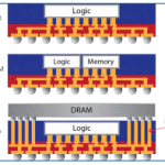
In constant pursuit of improved performance, power and cost, chip and system designers always want to integrate more functions together because this minimizes inter-device loads (affecting performance and power) and bill of materials on the board (affecting cost). However it generally isn’t possible to integrate … Read More
5 of the Top 20 Semiconductor Suppliers to Show Double-Digit Gains in 2016!
Semiconductor Market Researcher IC Insights released an update to the 2016 semiconductor sales forecast which is interesting on many different levels. It really has been an exciting year for the semiconductor industry, absolutely. Two of the stars of this year’s report happen to be two of my favorite fabless companies, Nvidia… Read More
Foundry CAPEX Jumped from 17% to 37% of LAM Business
Lam- in line qtr but guides above street over near term. As with ASML, foundry is driver with subdued memory, The Math implies biz peaking-Looking for DRAM in 2017.
Lam reported another great, record quarter, more or less in line with expectations with revenues coming in at $1.632B and shipments of $1.708B, generating EPS of $1.81.… Read More
Webinar Offers View into TSMC IP Design Methodology
Standard cell and memory IP are key enablers for new process node availability. These two items must be in place early and be completely ready for a process node to scale to volume. Development of both leaves no room for error and they require the highest performance possible. Foundries are extremely focused on this and spend a lot… Read More
Will TSMC be alone at 10nm and 7nm?!?!?
Now that the dust has settled let’s talk about the recent TSMC OIP Ecosystem Forum. This was the 6[SUP]th[/SUP] annual OIP which hosts more than 1,000 attendees from TSMC’s top customers and partners. Presenting this year were TSMC VP and CTO Dr. Jack Sun, TSMC VP of R&D Dr. Cliff Hou, and ARM EVP of Incubation Businesses Dr. Dipesh… Read More
Top 5 Highlights from the 2016 TSMC Open Innovation Platform Forum
Recently, TSMC conducted their annual Open Innovation Platform forum meeting in San Jose. Although TSMC typically eschews a theme for the forum, David Keller, EVT TSMC North America, used a phrase in his opening remarks that served as a foundation for the rest of the meeting – “celebrate the way we collaborate”.
The forum begins… Read More
ESL Architectural Power Estimation Support from TSMC — yes, TSMC
Electronic system level (ESL) modeling for system architecture exploration is rapidly gaining momentum. The simulation performance requirements for hardware/software co-design are demanding — an abstract model for SoC IP cores is required. Typically, soft IP will include a number of model configuration parameters.… Read More
TSMC 16nm, 10nm, 7nm, and 5nm Update!
Word on the street is that TSMC is on schedule with 16FFC, 10nm and 7nm, which is a very big deal for the fabless semiconductor ecosystem. As Scotten Jones has illustrated in the graphic below, for the first time in the history of the semiconductor industry a pure-play foundry (TSMC) will have the process lead over Intel. And this is… Read More