Why do I stalk the FPGA industry? Well, FPGAs are an important part of the fabless semiconductor ecosystem for two reasons: 1.) They enable very cost effective design starts which are the life’s blood of the semiconductor industry and 2.) FPGA prototyping allows designers to verify their designs before committing to silicon and… Read More

Xilinx Skips 10nm
At TSMC’s OIP Symposium recently, Xilinx announced that they would not be building products at the 10nm node. I say “announced” since I was hearing it for the first time, but maybe I just missed it before. Xilinx would go straight from the 16FF+ arrays that they have announced but not started shipping, and to the… Read More
Electromigration Analysis and FinFET Self-Heating
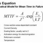
FinFET processes provide power, performance, and area benefits over planar technologies. Yet, a vexing problem aggravated by FinFET’s is the greater local device current density, which translates to an increased concern for signal and power rail metal electromigration reliability failures. There is a critical secondary… Read More
Is 7nm Coming to the TSMC OIP Ecosystem Forum?
This is the 5[SUP]th[/SUP] TSMC Open Innovation Platform Ecosystem Forum and it is not to be missed. Please note that the location has moved from the San Jose Convention Center to the Santa Clara Convention Center which is literally right across the street from the new Levi’s Stadium. If you haven’t been to the new stadium you really… Read More
Tackling Layout Gradient Effects in 16 nm FinFET using Layout Automation
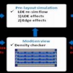
My first exposure to automating IC layout was back in the 1980’s at Intel where I coded a layout compiler to auto-generate about 6% of a graphics processor chip. The need to use automation for IC layout continues today, and with the advent of FinFET technology there are some new challenges like layout gradient effects that … Read More
Synopsys Vision on Custom Automation with FinFET

In an overwhelmingly digital world, there is a constant cry about the analog design process being slow, not automated, going at its own pace in the same old fashion, and so on. And, the analog world is not happy with the way it’s getting dragged into imperfect automation so it can be more like the digital world. True, the analog world… Read More
Samsung: the Journey to 14nm and 10nm
At the Samsung theatre (cutely named the Samsung Open Collaboration (SoC) theater) I watched a presentation by KK Lin on using DFM to bring up their 14nm and 10nm processes. And yes, they are real. Here is a picture I took of a 14nm wafer and a 10nm wafer. Samsung announced that they would ramp 10n to volume production by the end of next… Read More
TSMC Shows 10nm Wafer!
If you really want to know why I write about TSMC it is all about ego, my massive ego, absolutely. Blogs about TSMC and the foundries have always driven the most traffic and they most likely always will. Semiconductor IP is second, Semiconductor Design is third, and I don’t think that is going to change anytime soon:
SemiWiki BI: Daniel… Read More
Samsung Foundry Debuts 10nm Wafer!
The Samsung Smart, Connected Lifestyle event was last night at the Bently Reserve in San Francisco. Getting into San Francisco was no picnic with all of the roadwork and new building construction. We even saw people drive up on the sidewalk to get around car clogs. It really was crazy but definitely worth it after seeing the first … Read More
TCAD Enables Moore’s Law to Continue
We live in very interesting times, you can wear an Android watch from Samsung that uses 14 nm FinFET technology, attend the 52nd DAC conference in June to learn about EDA and IP vendors supporting FinFET, and read about research work for new devices down to 5 nm. TCAD is that critical software technology that enables the development… Read More
Quantum Simulation Using Decision Diagrams. Innovation in Verification