It is that time again, time for the originators of the pure-play foundry business to update their top customers and partners on the latest process technology developments and schedules. More specifically, all of the TSMC FinFET processes (16nm, 10nm, 7nm, and beyond), TSMC IP portfolio (CMOS image sensor, Embedded Flash, Power… Read More

FinFET For Next-Gen Mobile and High-Performance Computing!
Evolving opportunities call for new and improved solutions to handle data, bandwidth and power. Moving forward, what will be the high-growth applications that drive product and technology innovation? The CAGRs for smartphone and data center continue to be very strong and healthy. … Read More
Advanced Micro Device’s New Polaris FinFET-Based Architecture Could Open New Doors
It seems of late like there is an unlimited thirst for GPU performance at the right power efficiency. Whether it is deep learning, object recognition, artificial intelligence, simulations, VR or AR, the industry desperately needs GPU improvements. Many within the graphics industry would agree that a new era of graphics performance… Read More
FinFETs, Power Integrity and Chip/Package Co-design
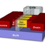
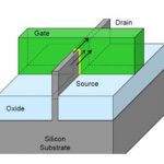
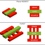
FinFETs have brought a lot of good things to design – higher performance, higher density and lower leakage power – promising to extend Moore’s law for a least a while longer. But inevitably with new advances come new challenges, especially around optimizing for power integrity in these designs.
One of these challenges is… Read More
How 16nm and 14nm FinFETs Require New SPICE Simulators
About 35 years ago the first commercial SPICE circuit simulators emerged and they were quickly put to work helping circuit designers predict the timing and power of 6um NMOS designs. Then we had to limit our circuit simulations to just hundreds of transistors and interconnect elements to fit into the RAM and complete simulation… Read More
2016 Samsung Foundry Update!
When sketching out the chapters for our book “Mobile UnLeashed” we sought out the events and technology that empowered the mobile devices that literally changed our world. One of the companies that enabled this change of course is Samsung. Cleverly embedded in chapter 8 “To Seoul, via Austin” is the story of how Samsung got into … Read More
Synopsys on the Future of Custom Layout!
Analog and mixed signal design has received more than their fair share of attention since the mobile revolution and now that FinFETs are in production at the foundries I see that trend continuing. As a result this year there are some interesting things brewing in EDA, especially in the area of Custom Layout.
Innovation in Custom … Read More
FinFET will finally arrive for GPU’s in 2016
It used to be that GPU chips moved to new process nodes pretty frequently, previously as often as annually. That is up until 2011. That was the year that 28nm GPU’s were unveiled. Since then there has been a long pause. Now in the wake of the 2016 CES both Nvidia, with its previously announced Pascal, and AMD, with the just announced Polaris,… Read More
Variation Aware FinFETs are Critical!

As I mentioned in “EDA Dead Pool” acquisitions in our industry will continue at a rapid pace. The latest victim is 10 year old French company Infiniscale who was recently purchased by Silvaco. This was more of a “let’s put your product through our massive sales and support channel” kind of deal so it will be 1 + 1 = 3 accretive for sure.… Read More
Are FinFETs too Expensive for Mainstream Chips?
One of the most common things I hear now is that the majority of the fabless semiconductor business will stay at 28nm due to the high cost of FinFETs. I wholeheartedly disagree, mainly because I have been hearing that for many years and it has yet to be proven true. The same was said about 40nm since 28nm HKMG was more expensive, which … Read More
TSMC CoWoS versus Intel EMIB Semiconductor Packaging