You are currently viewing SemiWiki as a guest which gives you limited access to the site. To view blog comments and experience other SemiWiki features you must be a registered member. Registration is fast, simple, and absolutely free so please,
join our community today!
WP_Term Object
(
    [term_id] => 50
    [name] => Events
    [slug] => events
    [term_group] => 0
    [term_taxonomy_id] => 50
    [taxonomy] => category
    [description] =>
    [parent] => 0
    [count] => 1557
    [filter] => raw
    [cat_ID] => 50
    [category_count] => 1557
    [category_description] =>
    [cat_name] => Events
    [category_nicename] => events
    [category_parent] => 0
    [is_post] =>
)
The TSMC Symposium kicked of today. I will share my general thoughts while Tom Dillinger will do deep dives on the technology side. The event started with a keynote by TSMC CEO CC Wei followed by technology presentations by the TSMC executive staff.
C.C. Wei introduced a new sound bite this year that really resonated with me and that… Read More
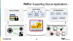
Throughout history, people have sought after security as a basic right and expectation within a civilized society. Even as recent as a few centuries ago, things were very simple. Subjects looked to their rulers to provide security for their lives and assets. Assets were mostly hard assets such as jewelry, coins or real estate. … Read More
Machine learning applications have become pervasive and increasingly complex, from recommendation agents in online interactions to personal assistants for command response to (ultimately) autonomous vehicle control. Yet, an often overlooked facet of machine learning technology is the deployment in industrial process… Read More
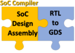
Defacto SoC Compiler whose 9.0 release was announced recently automates the SoC design creation from the first project specifications. It covers register handling, IP and connectivity insertion at RTL, UPF and SDC file generation right to logic synthesis. As part of the generation process of RTL and design collaterals, basic… Read More
The above title refers to a webinar that was hosted by Altair on April 28th. Chip design in the cloud is not a new idea. So, what is the big deal with the above title. Sometimes titles don’t reveal the full story. Annapurna Labs happens to be an Amazon company. It used to be an independent semiconductor company that was acquired by Amazon… Read More
A great deal has been written of late about the demise of Moore’s Law. The increase in field-effect transistor density with successive process nodes has slowed from the 2X every 2 1/2 years pace of earlier generations. The economic nature of Moore’s comments 50 years ago has also been scrutinized – the reduction in cost per transistor… Read More
When we think about Compute and AI SoCs, we often focus on the huge numbers of calculations being carried out every second, and the ingenious IPs that are able to reach such high levels of performance. However, there also exists a significant challenge in keeping the vast quantities of data flowing around the chip which is solved … Read More
This topic is inspired by a presentation at last year’s DAC presented by Methodics, now part of Perforce. The issues raised by the original presentation are still quite relevant in the current business climate. IP leakage is something everyone should consider as part of their normal business operations. Your design IP really … Read More
Engineers love to optimize their designs, but that implies that there are models and stimulus to automate the process. Process engineers have TCAD tools, circuit designers have SPICE for circuit simulation, logic designers have gate-level simulators, RTL designers use logic simulation, but what is there for the system architects… Read More
The Signal Integrity Journal recently held a half day Electronic Systems SI/PI Forum that included presentations from industry leaders covering key design topics for signal integrity and power integrity engineers. The event was sponsored by Cadence. The keynote for the event was presented by Istvan Novak, principal signal… Read More


Consolidation and Competition: Who is Winning the $4.5 Billion Interface IP Race?