
“What are the tradeoffs when designing a register file?” Engineering graduates pursuing a career in microelectronics might expect to be asked this question during a job interview. (I was.)
On the surface, one might reply, “Well, a register file is just like any other memory array – address inputs, data inputs and outputs, read/write operation cycles. Maybe some bit masking functionality to write a subset of the data inputs. I’ll just use the SRAM compiler for the foundry technology.” Alas, that answer will likely not receive any kudos from the interviewer.
At the recent International Solid State Circuits Conference (ISSCC 2021), TSMC provided an insightful technical presentation into their unique approach to register file implementation for the 5nm process node. [1]
The rest of this article provides some of the highlights of their decision and implementation tradeoffs. I would encourage SemiWiki readers to obtain a copy of their paper and delve more deeply into this topic (particularly before a job interview).
Register File Bitcell Implementation Options
There are three general alternatives for selecting the register file bit cell design:
- an array of standard-cell flip-flops, with standard cell logic circuitry for row decode and column mux selection

The figure above illustrates n registers built from flip-flops, with standard logic to control the write and read cycles (shown separately above) – one write port and two read ports are shown.
- a conventional 6T SRAM bitcell

The figure above illustrates an SRAM embedded within a stdcell logic block, where the supply voltage domains are likely separate. Additional area around the SRAM is required, to accommodate the difference between the conventional cell layout rules and the “pushed” rules for (large) SRAM arrays.
- a unique bitcell design, optimized for register file operation

For the 5nm register file compiler, TSMC chose the third option using the bitcell illustrated above, based on the considerations described below. Note that the 16-transistor cell includes additional support for masked bit-level write, using the additional CL/CLB inputs. The TSMC team highlighted that this specific bit-write cell design reduces the concern with cell stability for adjacent bitcells on the active wordline that are not being written – the “half-select” failure issue (wordline selected, bit column not selected).
Bitcell Layout
The foundry SRAM compiler bitcell typically uses unique (aggressive) layout design rules, optimized for array density. Yet, there are specific layout spacing and dummy shape transition rules between designated SRAM macros and adjacent standard cell logic – given the large number of register files typically present in an SoC architecture, this required transition area is inefficient.
Flip-flops use the conventional standard cell design layout rules, with fewer adjacency restrictions to adjacent logic.
For the TSMC 5nm register file bitcell, standard cell digital layout rules were also used.
Peripheral Circuitry
A major design tradeoff for optimal register file PPA is the required peripheral circuitry around the bitcell array. There are several facets to this tradeoff:
- complexity of the read/write access cycle
The flip-flop implementation shown above is perhaps the simplest. All flip-flop outputs are separate signals, routed to multiplexing logic to select “column” outputs for a read cycle. Yet, the wiring demand/congestion and peripheral logic depth grows quickly with the number of register file rows.
The SRAM uses dotted bitcell inputs and outputs along the bitline column; the decoded row address is the only active circuit on the bitline. A single peripheral write driver and differential read sense circuit supports the entire column.
The TSMC register file bitcell also adopts a dotted connection for the column, but separates the write and read bit lines. The additional transistors comprising the read driver in the cell (P6, N6, P7, and N7 in the bitcell figure above) offer specific advantages:
- the read output is full-swing, and static (while the pass gate N7/P7 is enabled)
No SRAM differential bitline precharge/discharge read access cycle is needed, saving power. The read operation does not disturb the internal, cross-coupled nodes of the bitcell.
- the read and write operations are independent
The use of separate WWL and RWL controls allows a concurrent write operation and read operation to the same (“write-through”) or different row.
Although based on digital standard cell design rules, note that the peripheral circuitry for the TSMC register file design needs some special consideration. The read output transfer gate circuit presents a diffusion node at the bitcell boundary, with multiple dotted bitcell rows. This node is extremely sensitive to switching noise, and requires detailed analysis.
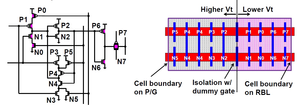
Vt Selection
The choice of standard cell design rules also allows greater flexibility for the TSMC register file bitcell. For example, low Vt devices could be selectively used in the read buffer for improved performance, with a minor impact on bitcell leakage current, as illustrated below.

VDD Operation
Perhaps the greatest register file implementation tradeoff pertains to the potential range of operating supply voltages available to foundry customers. At advanced process nodes, the range of supply voltages needed for different target markets has increased. Specifically, very low power applications require aggressive reductions in VDDmin – e.g., for the 5nm process node, logic functionality down to ~0.4-0.5V (from the nominal VDD=0.75V) is being pursued.
The use of standard cell design rules enables the register file implementation to scale the supply voltage with the logic library – indeed, the embedded register file can be readily integrated with other logic in the block in a single power domain.
Conversely, the traditional SRAM cell design at advanced nodes increasingly requires a “boost” during the write operation, to ensure sufficient design margin across a large number of memory bitcells, using aggressive design rules. This write assist cycle enables a reduction in the static SRAM supply voltage, reducing the SRAM leakage current. Yet, it also introduces considerable complexity to the access cycle with the charge-pump boost precursor (possibly even requiring a read-after-write operation to confirm the written data).
Write Power
Another comparison to a conventional SRAM bitcell worth mentioning is that the feedback loop in the TSMC register file bitcell is broken during the write operation. (Most flip-flops circuits also use this technique.) The write current overdrive used to flip the state of the SRAM bitcell with cross-coupled inverters dissipates greater power during this cycle.
Testsite and Measurement Data
The first figure below shows the 5nm register file testsite photomicrograph, with two array configurations highlighted. The second figure illustrates the measured performance data for 4kb and 8kb register file macros, across VDD and temperature ranges. Note the selection of a digital process design enables functional operation down to a very low VDDmin.
(Astute observers will note the nature of temperature inversion in the figure – operation at 0C is more limited than at 100C.)


The testsite macros also included DFT and BIST support circuitry – the test strategy (and circuit overhead) is definitely part of the register file implementation tradeoff decision.
Summary: The Final Tradeoff
Like all tradeoffs, there is a range of applicability which much be taken into account. for the case of register file implementation using either flip-flops, conventional SRAM bitcells, or a unique bitcell as developed by TSMC for the 5nm node, the considerations are:
- area: dense 6T SRAM cells with complex peripheral circuitry versus larger area cells (using digital design rules)
- VDDmin support (power) and VDDmax capabilities (performance, reliability)
- masked bit-write requirements
- test methodology (e.g., BIST versus a simple scan chain through flip-flops)
- and, last but certainly not least,
- number of register file access ports (including concurrent read/write operation requirements)
The TSMC focus for their ISSCC presentation was on a 1W, 1R port architecture. If more register file ports are needed, the other tradeoff assessments listed above change considerably.
The figure below illustrates the area tradeoff between an SRAM bitcell and the 5nm bitcell, indicating a “cross-over” point at ~40 rows (for 256 columns). The 4kb (32×128) and 8kb (32×256) register file macros shown earlier fit with the preferred window for the fully digital bitcell design.

For reference, TSMC also shared this tradeoff for their previous 7nm register file design, as shown below (1W1R ports). [2] Note the this figure also includes the lower range, where a flip-flop-based implementation is attractive.

Yet, as currently SoC architectures demand larger on-die local storage, the unique bitcell design in 5nm supporting optimum 4kb and 8kb macros hits the sweet spot.
Hopefully, this article will help you nail the register file design job interview question. 🙂
I would encourage you to read the TSMC papers describing their design approach and tradeoff assessments on 5nm (and 7nm) register file implementations.
-chipguy
References
[1] Fujiwara, H., et al., “A 5nm 5.7GHz@1.0V and 1.3GHz@0.5V 4kb Standard-Cell-Based Two-Port Register File with a 16T Bitcell with No Half-Selection Issue”, ISSCC 2021, paper 24.4.
[2] Sinangil, M., et al., “A 290mV Ultra-Low Voltage One-Port SRAM Compiler Design Using a 12T Write Contention and Read Upset Free Bitcell in 7nm FinFET Technology”, VLSI Symposium 2018.
Share this post via:


Comments
There are no comments yet.
You must register or log in to view/post comments.