The EDA Consortium (EDAC) has changed name for Electronic Systems Design Alliance (ESD Alliance). That’s a good reminder that IC are developed (thanks to Design Automation) to be integrated into a System. A wide design ecosystem support system development, including embedded software, design intellectual property (IP), … Read More

Electronic Design Automation
“Thinking Outside the Chip”
While pushing Moore’s Law’s boundaries in the world of 2D packaging, companies are starting to explore nontraditional approaches towards designing integrated circuit chips. 2D packaging is currently the most used method in designing chips in the industry, and while it leads in efficiency of power and performance, it lacks … Read More
Making PLM Actually Work for for IC Design
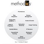
The topic of Product Lifecycle Management (PLM) conjures up images of usage on airplanes, tanks and cars. That’s because it was developed decades ago to help make product development and delivery more efficient for big expensive manufactured products. It worked well for its intended markets by combining and managing all the … Read More
Neural Networks Poised to Make Big Changes in Our World

Probably the most interesting thing about Neural Networks is how they can be used for complex recognition tasks that we as people can easily perform but we might have a lot of trouble explaining how. One very good example of a problem that Neural Networks can tackle is determining when people are making a fake smile. Intuitively we… Read More
Custom Layout Productivity Gets a Boost
In the 1970’s, when Moore’s Law was still in its infancy, Bill Lattin from Intel published a landmark paper [1]. In it he identified the need for new design tools and methods to improve layout productivity, which he defined as the drawn and verified number of transistors per day per layout designer. He said existing … Read More
The Importance of Transistor-Level Verification
According to the IEEE Std 1012-2012, verification is the acknowledgement that a product is in satisfactory condition by meeting a set of rigorous criteria. [3] Transistor-level verification involves the use of custom libraries and design models to achieve ultimate performance, low power, or layout density. [2] Prediction… Read More
Webinar alert – Taking UVM to the FPGA bank

UVM has become a preferred environment for functional verification. Fundamentally, it is a host based software simulation. Is there a way to capture the benefits of UVM with hardware acceleration on an FPGA-based prototyping system? In an upcoming webinar, Doulos CTO John Aynsley answers this with a resounding yes.… Read More
3D TCAD Simulation of Silicon Power Devices
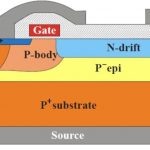
Process and device engineers are some of the unsung heroes in our semiconductor industry that have the daunting task of figuring out how to actually create a new process node that will fit some specific, market niche with sufficient yield to make their companies profitable and stand out from the competition. One such market segment… Read More
The Most Important Point You May Have Missed at CDNLive 2016!

This was the best keynote lineup I can remember at a user group meeting. All four speakers are visionaries but from very different perspectives. The video of the event will be up later this month but from my first count the word “System(s)” was mentioned 32 times and the underlying message will transform the semiconductor industry… Read More
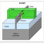
Innovation in Transistor Design with Carbon Nanotubes
The New York Times article “IBM Scientists Find New Way to Shrink Transistors” by John Markoff focuses on the goal of the semiconductor industry to create smaller transistors in order to remain competitive while emphasizing cutting-edge design strategies with the use of carbon nanotubes. By switching from traditional methods… Read More
Intel: Pushing EMIB Forward: Design Methodology Insights with Synopsys Tools