
For many year 2D NAND drove lithography for the semiconductor industry with the smallest printed dimensions and yearly shrinks. As 2D NAND shrunk down to the mid-teens nodes, 16nm, 15nm and even 14nm, the cells became so small that there were only a few electrons in each cell and cross-talk issues made further shrinks very difficult… Read More

Author: Scotten Jones
Samsung Details Foundry Roadmap
Samsung recently held a meeting where they laid out a detailed roadmap for their foundry business. On Tuesday June 1st, Daniel Nenni and myself had an interview with Kelvin Low, senior director of foundry marketing and business development to discuss the details of Samsung’s plans.… Read More
SPIE 2017 – imec papers and interview
At the SPIE Advanced Lithography Conference imec published a number of papers on EUV, multi-patterning and other lithography issues. In addition to seeing several of the papers presented I had a chance to sit down with imec’s director of advanced patterning, Greg McIntyre. In this article I will summarize my discussions… Read More
SPIE 2017 – ASML Interview and Presentations
At the SPIE Advanced Lithography conference I sat down with Mike Lercel, Director of Strategic Marketing for ASML for an update. ASML also presented several papers at the conference and I attended many of these. In this article, I will discuss my interview with Mike and summarize the ASML presentations.… Read More
SPIE 2017 ASML and Cadence EUV impact on place and route
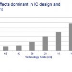
As feature sizes have shrunk, the semiconductor industry has moved from simple, single-exposure lithography solutions to increasingly complex resolution-enhancement techniques and multi-patterning. Where the design on a mask once matched the image that would be produced on the wafer, today the mask and resulting image … Read More
SPIE 2017: Irresistible Materials EUV Photoresist
Irresistible Materials (IM) is a spin-out of the University of Birmingham in the United Kingdom that has been doing research on Photoresist and Spin-On Carbon hard masks for 10 years, most recently with Nano-C on chemistry development. IM has developed a unique EUV photoresist and they are now looking for partners to help bring… Read More
14nm 16nm 10nm and 7nm – What we know now
Last week Intel held a manufacturing day where they revealed a lot of information about their 10nm process for the first time and information on competitor processes continues to slowly come out as well. I thought it would be useful to summarize what we know now, especially since some of what Intel announced was different than what… Read More
Shootout at 22nm!
For an industry that drives improvement at an exponential rate it is funny how often something old is new again. Intel went into high volume production on 22nm in 2011, and TSMC and Samsung have both had 20nm technologies in production for several years. And yet, recently we have seen renewed interest in 22nm. GLOBALFOUNDRIES has… Read More
Intel Manufacturing Day: Nodes must die, but Moore’s Law lives!
Yesterday I attended Intel’s manufacturing day. This was the first manufacturing day Intel has held in three years and according to Intel their most in depth ever.
Nodes must die
I have written several articles comparing process technologies across the leading-edge logic producers – GLOBALFOUNDRIES, Intel, Samsung… Read More
SPIE 2017: EUV Readiness for High Volume Manufacturing
The SPIE Advanced Lithography Conference is the world’s leading conference addressing photolithography. This year on the opening day of the conference, Samsung and Intel presented papers summarizing the readiness of EUV for high volume manufacturing (HVM). In this article, I will begin by summarizing the EUV plans … Read More


TSMC CoWoS versus Intel EMIB Semiconductor Packaging