You are currently viewing SemiWiki as a guest which gives you limited access to the site. To view blog comments and experience other SemiWiki features you must be a registered member. Registration is fast, simple, and absolutely free so please,
join our community today!
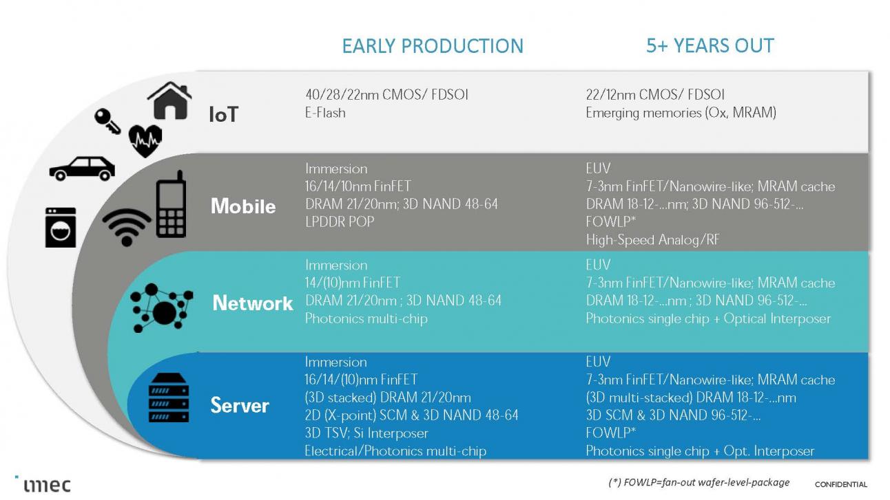
At the IEDM 2017, imec held an imec technology forum and presented several papers, I also had the opportunity to interview Anda Mocuta director of technology solutions and enablement. In this article I will summarize the keys points of what I learned about the future of logic. I will follow this up with a later article covering memory.… Read More
As I have discussed in previous blogs, IEDM is one of the premier conferences to learn about the latest developments in semiconductor technology. … Read More
“Mobile is the largest platform ever built by humanity”, Christiano Amon, Executive Vice President, Qualcomm Technologies, Inc. and President, Qualcomm CDMA Technologies speaking at the GLOBALFOUNDRIES Technologies Conference (GTC) 2017.… Read More
The 63rd annual IEDM (International Electron Devices Meeting) will be held December 2nd through 6th in San Francisco. In my opinion IEDM is one of, if not the premier conference on leading edge semiconductor technology. I will be attending the conference again this year and providing coverage for SemiWiki. As a member of the press… Read More
On September 20th GLOBALFOUNDRIES (GF) held their annual technology conference. The conference presented an opportunity to hear the latest on the fascinating journey GF has been on.… Read More
At the imec technology forum held at SEMICON West, Martin Van Den Brink, President and CTO of ASML presented on the latest developments on EUV. I also had an opportunity to sit down with Mike Lercel, ASML Director of Strategic Marketing for an interview.… Read More
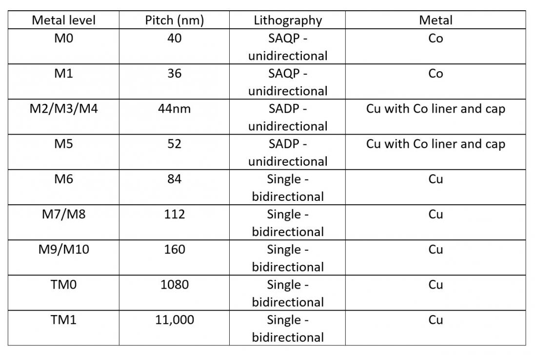
At SEMICON West I attended the imec technology forum where Zsolt Tokei presented “How to Solve the BEOL RC Dilemma” and the SEMICON Economics of Density Scaling session where Larry Clevenger of IBM presented “Interconnect Scaling Strategic for Advanced Semiconductor Nodes”. I also had the opportunity… Read More
At Semicon West last week I attended presentations by Soitec and CEA Leti, and had breakfast with CEA Leti CEO Marie Semeria, key members of the Fully Depleted Silicon On Insulator (FDSOI) ecosystem. I have also seen some comments in the SemiWiki forum lately that make me believe there is some confusion on the roles of different companies… Read More
I have previously published analysis’ converting leading edge logic processes to “standard nodes” and comparing standard nodes by company and time. Recently updated details on the 7nm process node have become available and in this article, I will revisit the standard node calculations and trends.… Read More
In a SemiWiki EXCLUSIVE – GLOBALFOUNDRIES has now disclosed the key metrics for their 7nm process. As I previously discussed in my 14nm, 16nm, 10nm and 7nm – What we know now blog GLOBALFOUNDRIES licensed their 14nm process from Samsung and decided to skip 10nm because they thought it would be a short-lived node. At … Read More


TSMC CoWoS versus Intel EMIB Semiconductor Packaging