On September 20th GLOBALFOUNDRIES (GF) held their annual technology conference. The conference presented an opportunity to hear the latest on the fascinating journey GF has been on.
To recap briefly, GF was initially a set of fabs spun out from AMD. GF then bought the Chartered Semiconductor Foundry and eventually took over IBM’s semiconductor manufacturing operations. Prior to the IBM acquisition GF had been plagued with execution issues. At 14nm GF was late developing their own process and they were forced to license a 14nm process from Samsung. The IBM acquisition added 500 researchers to GF and GF has been developing their own 7nm FinFET process. IBM also brought a portfolio of RF processes and SOI expertise. GF is now one of two foundries pursuing FDSOI technology.
The Semiconductor Opportunity
Sanjay Jha, the CEO of GF opened the conference with his keynote address. In his keynote Sanjay stated that he believes we are entering a new golden age of semiconductors and that over the next 10 to 20 years autonomous driving and AR/VR will drive the market. He noted that the volume of pictures being taken is exploding and that so much data is being generated that we need local processing before communicating to the cloud. He believes 5G will disrupt communications the way the switch from voice to data did. We are going to transition from 1MB/sec to 1GB/sec with 5G.
Christiano Amon, Executive Vice President, Qualcomm Technologies, Inc. and President, Qualcomm CDMA Technologies followed Sanjay and made his own bullish statements stating that semiconductors best years are still ahead of us. “Mobile is the largest platform ever built by humanity. There are more smart phones than toothbrushes”. Cristiano further stated that over $12 trillion dollar in 5G related goods and services are expected in 2035 as the unifying fabric for mobile, automotive and IOT. There are $3 billion dollars per year of rapidly growing opportunities by bringing mobile to industries that aren’t mobile, for example automotive.
Execution
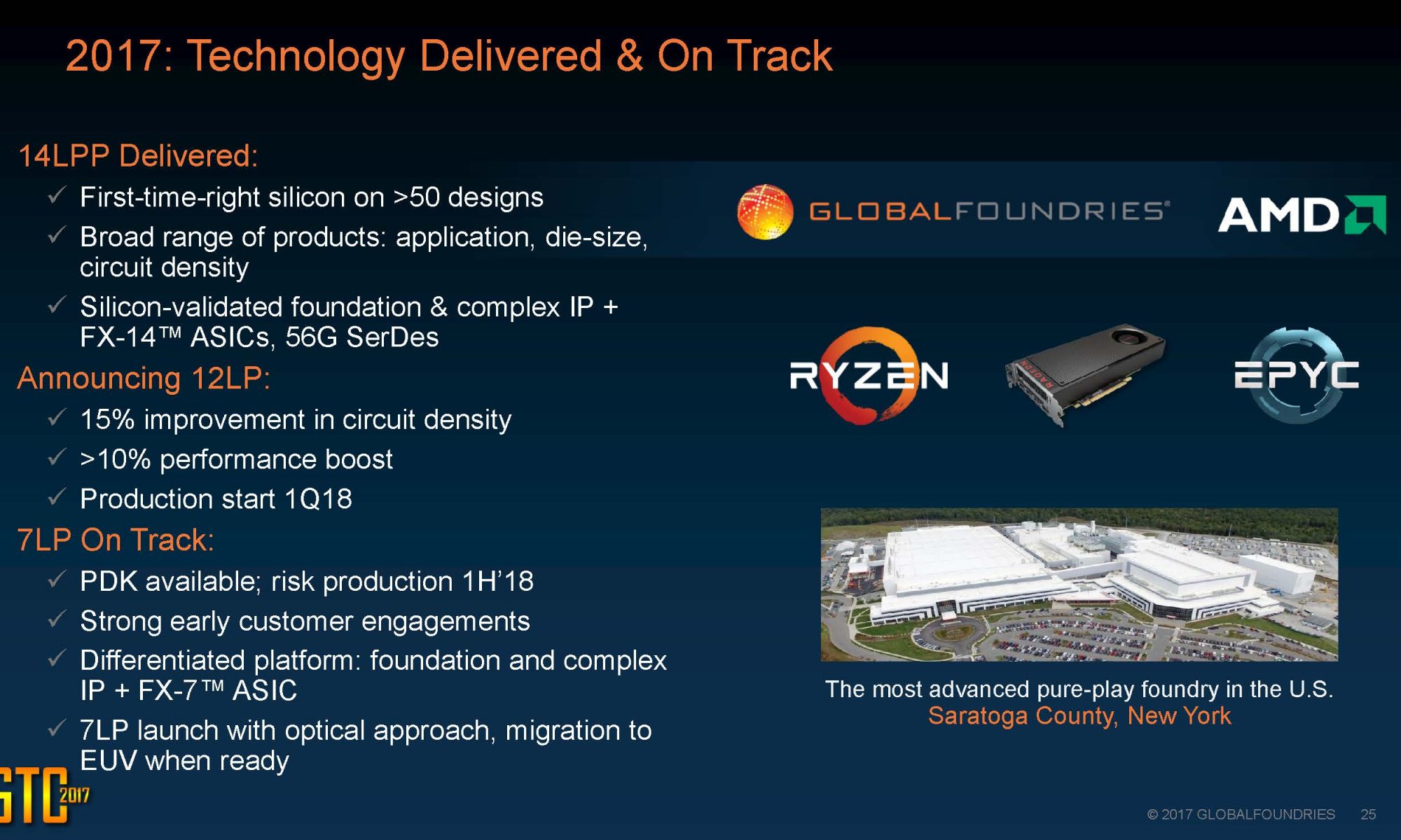
As I noted in my opening paragraph GF was at one time plagued by execution issues. Since the IBM semiconductor acquisition GF has been delivering on all their milestones with the development of their 7LP 7nm technology and 22FDX FDSOI technology. Figure 1 is a slide GF presented on their 2017 accomplishments.
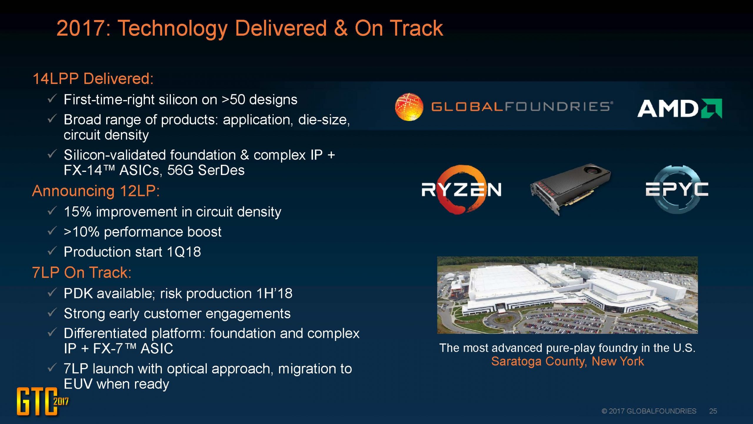
Figure 1. GF 2017 Accomplishments.
During his keynote Sanjay called some of GF’s customers up to the stage to discuss their performance.
Mark Papermaster, CTO and senior vice president at AMD characterized GF’s execution on this newly announced 12LP process as “outstanding” and stated that AMD was moving into 12LP for 2018.
Todd Gillenwater, CTO and Vice President of Mobile Engineering at Qorvo talked about working with IBM and now GF for ten years. They launched RF SOI in 2010 and also use SiGe. SiGe is an older technology but they are still finding “more legs in it”. Authors note I will be publishing a comprehensive article on GF’s RF technologies including SiGe soon.
Joel King, Vice President and General Manager of Advanced Mobile at Skyworks also took the stage to compliment GF’s technologies.
Sanjay noted that Dream Chip has delivered the first ADAS and IEDA has introduced 12 System-On-Chip (SOC) designs for IOT and they were all done on GF’s 22FDX platform.
Gary Patton, CTO and Senior Vice President at GF also discussed GF’s execution to schedule on their new processes (more on that in the next section). GF has now delivered >50 first time right designs on 14LPP.
Technology Update
GF has the most aggressive FDSOI roadmap in the industry with their 22FDX process ramping now and 12FDX in development. 22FDX and 12FDX are targeted at IOT, mobile and RF applications and offer FinFET like performance at lower cost. The thin silicon device layer and thin buried oxide layer of FDSOI enable body biasing to be used to tune performance and power consumption. GF picked 22nm and 12nm as their technology nodes to limit multi-patterning and provide lower costs. 22FDX has 40% less masks than 14nm FinFET and 12FDX has 40% less masks than 10nm/7nm FinFET. For large chips FDSOI can’t compete with FinFETs but for smaller chips FDX offers lower cost, lower power and better analog and RF performance. 22FDX was qualified in March of 2017 and is approaching 28nm mature yields. PDK 1.2 has been delivered along with validated design flows and IP. GF is building up 1.5 million wafers per year of capacity between Dresden and the new Chengdu China fab. Figure 2 illustrates the current status of 22FDX.
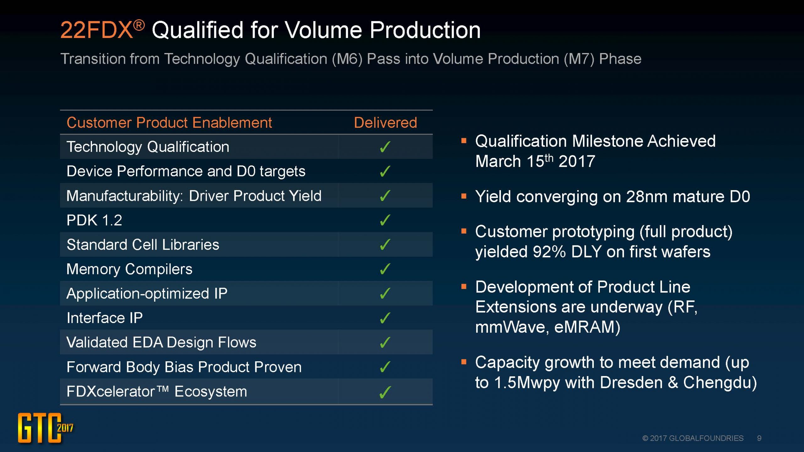
Figure 2. 22FDX Status.
I often get asked whether I think FDSOI will really take off and my answer is that I do think it will take off for IOT and other mobile applications. GF reported they now have 135 early engagements, 102 PDK downloads, 72 Invecas IP downloads and there will be 20 test designs on multi product wafers by the end of 2017 with 15 product tape-outs by the end of 2018.
12FDX is in development and expected to provide 26% better performance and 47% lower power than 22FDX. 12FDX will have a minimum energy point of <0.4 volts well below what FinFETs can offer. Samsung is the only other foundry pursuing FDSOI and their process nodes are 28nm currently with 18nm in development, both less dense than GF’s competing 22nm and 12nm offerings.
7LP (Leading performance) is GF’s leading edge 7nm FinFET process. Whereas GF licensed Samsung’s FinFET process at 14nm, at 7nm GF is developing their own process. Device performance at 7nm is >40% better than at 14nm and total power is >60% lower than 14nm. 7nm will provide 17 million gates/mm[SUP]2[/SUP]and a 30% die cost reduction versus 14nm with a >45% cost reduction for target segments. The PDK is available now and risk production is on track for the first half of 2018. Figure 3 presents the 7LP platform.
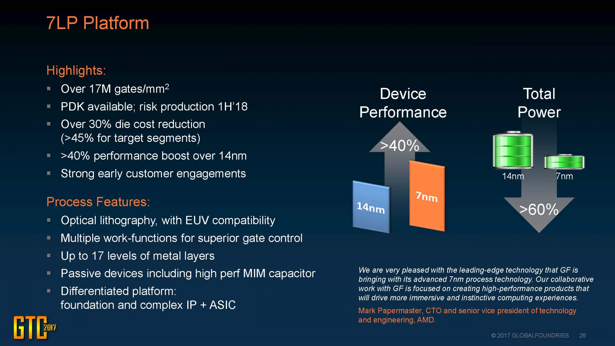
Figure 3. 7LP Platform
The initial 7nm process will be optical with an EUV version planned for when EUV is ready (more on EUV shortly).
GF also offers an FX-7 ASIC services utilizing the 7LP process.
Other new announcements at the conference:
- 55nm BCDLite adds analog and power devices to the 55LP platform. Isolated EDNMOS and EDPMOS, TaN resistors, high resistance resistors, zener diodes and MIM caps, 5 to 8 metals layers and a thick top metal are options.
- 12LP (leading performance) is a mid-life kicker for 14nm and offers 15% greater density and 10% better performance. 12LP is designed to be competitive with other 12nm foundry processes (TSMC recently announced a 12nm process and Samsung announced an 11nm process). Production is due to start in Q1-2018.
- 8SW is an RFSOI process on 300mm wafers for front end modules targeting 4G LTE and sub 6GHz 5G applications. It offers 70% lower power than the previous generation and will be produced in the Fab 10 East Fishkill fab.
- 14HP (high performance) is a 14nm FinFET on SOI process produced exclusively for IBM. 14HP offers 17 metal layers and a trench capacitor embedded DRAM. What is notable here is 14HP has been moved out of East Fishkill into the Malta fab and East Fishkill is now focused on 300mm RF SOI and Silicon Photonics.
- Embedded MRAM is now available for the 22FDX platform and provides 10-year data retention at 125[SUP]o[/SUP]C and is compatible with 260[SUP]o[/SUP]C solder reflow. Embedded MRAM will roll out to other GF processes over time.
In terms of EUV status:
- Source – delivering >125 wafers per hour with >80% uptime. ASML routinely sees >205 watts.
- Photoresist – trade-off between productivity and yield, it needs to get better.
- Masks/pellicles – mask yields are 65% versus 95% overall with defects in the mask build and the fab. There is currently no pellicle that works at 205 watts and you lose 30% of the light. Pellicle transmission loss needs to be <10%.
GF’s EUV plan is to introduce EUV on a second generation 7nm process for contacts and vias, due to the low open area of contacts and vias EUV can be implemented without a pellicle. Once a pellicle is available with <10% transmission loss then EUV will be used for Mx and Vx levels.
GF has a lot of expertise in advanced packaging but they are strictly development and move the designs to offshore partners for production. Packaging technologies include organic laminate/interposers, silicon interposers for 2.5D and direct 3D attach.
GF also offers a silicon photonics platform with gratings/couplers, active RFCMOS, waveguides, germanium detectors, active modulators and fiber edge coupler options. All of the silicon photonics modules have been demonstrated in a standards silicon foundry.
Working with their partners IBM and Samsung GF have demonstrated lateral nanowires/nanosheets for post FinFET process adoption beyond 5nm.
Design Enablement
With today’s leading-edge processes getting more complex to design for, design enablement is a key part of any foundry offering. This is particularly important with the new FDSOI processes 22FDX and 12FDX that offer back biasing for performance and power tuning where designers haven’t previously had to deal with back bias.
GF is investing heavily in design solutions and targeting first source solutions for 14LPP and 7LP and differentiated solutions with 22FDX, 12FDX, RFSOI and SiGe. GF is focused on reliable design enablement over the process life cycle. Early availability of IP, comprehensive design solutions and customer design productivity and design-to-sample cycle time. Figure 4 illustrates the continuing improvement in PDK quality at GF.
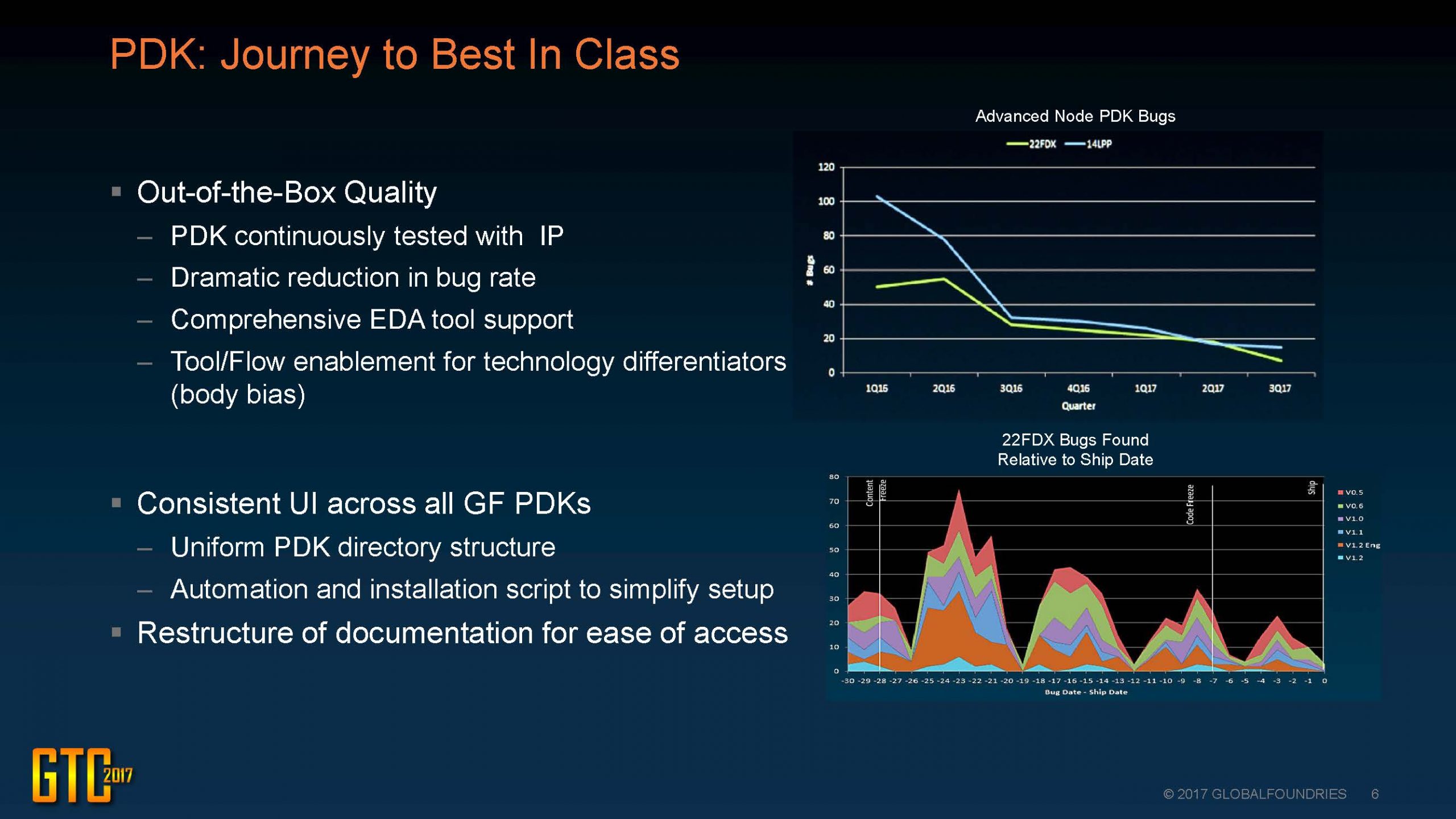
Figure 4. PDK Quality.
GF has certified reference flows available with both Synopsys and Cadence including FDSOI aware for 22FDX, see figure 5.
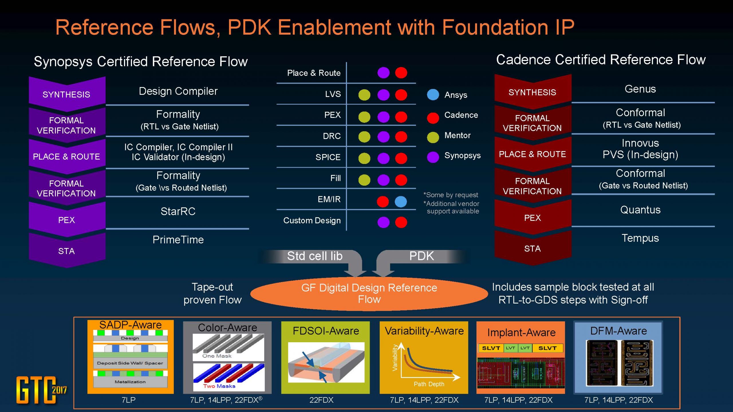
Figure 5. GF PDK Enablement.
GF is working with Arm, Synopsys, SiDense, eMemory, Kilopass, Attopsemi, Everspin and invecas on IP availability. An ARM Cortex-A53 produced in 22FDX shows a 25% reduction in area, a 42% reduction in power consumption and a 54% improvement in performance using biasing versus a 28nm design.
Key RF circuits are continuously evaluated and the results are fed back into PDK development as early as 0.1PDK.
Conclusions
GF is now demonstrating execution across the board on their roadmaps and the industry is noticing. GF’s process portfolio includes competitive leading edge FinFET processes in 14LPP and 7LP and industry leading RFSOI and SiGe solutions for RF. The new 22FDX FDSOI platform appears well positioned for the emerging IOT space with the 12FDX process in development for future extensions.
GF is now a viable leading foundry from a technology and execution standpoint. The next steps for GF will be to achieve profitability and demonstrate a sustainable financial model for the future.
Share this post via:


Solving the EDA tool fragmentation crisis