You are currently viewing SemiWiki as a guest which gives you limited access to the site. To view blog comments and experience other SemiWiki features you must be a registered member. Registration is fast, simple, and absolutely free so please,
join our community today!
Recent articles have focused much effort on studying the stochastic behavior of secondary electron exposure of EUV resists [1-4]. Here, we consider the implications of extending similar treatments to DUV lithography.
Basic Model Setup
As before, the model uses pixel-by-pixel calculations of absorbed photon dose, followed… Read More
Extreme ultraviolet (EUV) lithography is often represented as benefiting from the 13.5 nm wavelength (actually it is a range of wavelengths, mostly ~13.2-13.8 nm), when actually it works through the action of secondary electrons, electrons released by photoelectrons which are themselves released from ionization by absorbed… Read More
High-NA EUV lithography is the anticipated new lithography technology to be introduced for the 2nm node. Essentially, it replaces the 0.33 numerical aperture of current EUV systems with a higher 0.55 numerical aperture (NA). This allows the projection of smaller spot sizes and smaller pitches, roughly 60% smaller compared … Read More
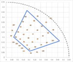
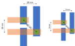
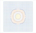
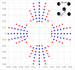
With metal interconnect pitches shrinking in advanced technology nodes, the center-to-center (C2C) separations between vias are also expected to shrink. For a 5/4nm node minimum metal pitch of 28 nm, we should expect vias separated by 40 nm (Figure 1a). Projecting to 3nm, a metal pitch of 24 nm should lead us to expect vias separated… Read More
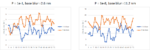
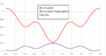
In the assessment of wafer lithography processes, normalized image log-slope (NILS) gives the % change in width for a given % change in dose [1,2]. A nominal NILS value of 2 indicates 10% change in linewidth for 10% change in dose; the % change in linewidth is inversely proportional to the NILS. In a previous article [2], it was shown… Read More
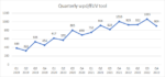
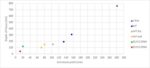
At the 2023 SPIE Advanced Lithography and Patterning conference, ASML presented an update on its EUV lithography systems in the field [1]. The EUV wafer exposure output was presented and is shown below in table form:
From this information, we can attempt to extract and assess the EUV wafer output per quarter. First, since there … Read More
Current 1a-DRAM and 5/4nm foundry nodes have minimum pitches in the 28 nm pitch range. The actual 28 nm pitch patterns are one-dimensional active area fins (for both DRAM and foundry) as well as one-dimensional lower metal lines (in the case of foundry). One can imagine that, for a two-dimensional routing pattern, both horizontal… Read More
Extreme ultraviolet (EUV) lithography systems are the most advanced lithography systems in use today. This article is a basic primer on this important yet complex technology.
The Goal: A Smaller Wavelength
The introduction of 13.5 nm wavelength continues a trend the semiconductor industry had been following a wavelength reduction… Read More
Masks have always been an essential part of the lithography process in the semiconductor industry. With the smallest printed features already being subwavelength for both DUV and EUV cases at the bleeding edge, mask patterns play a more crucial role than ever. Moreover, in the case of EUV lithography, throughput is a concern, … Read More
The “1.xnm” node on most roadmaps to indicate a 16-18 nm metal line pitch [1]. The center-to-center spacing may be expected to be as low as 22-26 nm (sqrt(2) times line pitch). The EXE series of EUV (13.5 nm wavelength) lithography systems from ASML feature a 0.55 “High” NA (numerical aperture), targeted… Read More


TSMC CoWoS versus Intel EMIB Semiconductor Packaging