
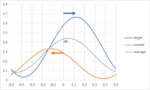
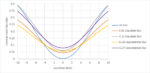
Normalized image log-slope (NILS) is probably the single most essential metric for describing lithographic image quality. It is defined as the slope of the log of intensity, multiplied by the linewidth [1], NILS = d(log I)/dx * w = w/I dI/dx. Essentially, it gives the % change in width for a given % change in dose. This is particularly… Read More

Author: Fred Chen
Can Attenuated Phase-Shift Masks Work For EUV?
Lithography Resolution Limits: The Point Spread Function
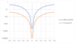
The point spread function is the basic metric defining the resolution of an optical system [1]. A focused spot will have a diameter defined by the Airy disk [2], which is itself a part of the diffraction pattern, based on a Bessel function of the 1st kind and 1st order J1(x), with x being a normalized coordinate defined by pi*radius/(0.5… Read More
Resolution vs. Die Size Tradeoff Due to EUV Pupil Rotation
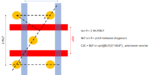
The many idiosyncrasies of EUV lithography affect the resolution that can actually be realized. One which still does not get as much attention as it should is the cross-slit pupil rotation [1-3]. This is a fundamental consequence of using rotational symmetry in ring-field optical systems to control aberrations in reflective… Read More
Multiple Monopole Exposures: The Correct Way to Tame Aberrations in EUV Lithography?
For a leading-edge lithography technology, EUV (extreme ultraviolet) lithography is still plagued by some fundamental issues. While stochastically occurring defects probably have been the most often discussed, other issues, such as image shifts and fading [1-5], are an intrinsic part of using reflective EUV optics. However,… Read More
Application-Specific Lithography: Sub-0.0013 um2 DRAM Storage Node Patterning
The pursuit of ever smaller DRAM cell sizes is still active and ongoing. DRAM cell size is projected to approach 0.0013 um2 for the D12 node. Patterning challenges are significant whether considering the use of DUV or EUV lithography. In particular, ASML reported that when center-to-center values reached 40 nm, single patterning… Read More
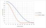
Secondary Electron Blur Randomness as the Origin of EUV Stochastic Defects

Stochastic defects in EUV lithography have been studied over the last few years. For years, the Poisson noise from the low photon density of EUV had been suspected [1,2]. EUV distinguishes itself from DUV lithography with secondary electrons functioning as intermediary agents in generating reactions in the resist. Therefore,… Read More
Predicting EUV Stochastic Defect Density
Extreme ultraviolet (EUV) lithography targets patterning pitches below 50 nm, which is beyond the resolution of an immersion lithography system without multiple patterning. In the process of exposing smaller pitches, stochastic patterning effects, i.e., random local pattern errors from unwanted resist removal or lack … Read More
Electron Blur Impact in EUV Resist Films from Interface Reflection
The resolution of EUV lithography is commonly expected to benefit from the shorter wavelengths (13.2-13.8 nm) but in actuality the printing process needs to include Pde the consideration of the lower energy electrons released by the absorption of EUV photons. The EUV photon energy itself has a nominal energy range of 90-94 eV,… Read More
Where Are EUV Doses Headed?
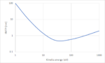
In spite of increasing usage of EUV lithography, stochastic defects have not gone away. What’s becoming clearer is that EUV doses must be managed to minimize the impact from such defects. The 2022 edition of the International Roadmap for Devices and Systems has updated its Lithography portion [1]. An upward trend with decreasing… Read More
Application-Specific Lithography: 5nm Node Gate Patterning
It has recently been revealed that the N5 node from TSMC has a minimum gate pitch of 51 nm [1,2] with a channel length as small as 6 nm [2]. Such a tight channel length entails tight CD control in the patterning process, well under 0.5 nm. What are the possible lithography scenarios?
Blur Limitations for EUV Exposure
A state-of-the-art


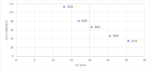
TSMC CoWoS versus Intel EMIB Semiconductor Packaging