Extreme ultraviolet (EUV) lithography is often represented as benefiting from the 13.5 nm wavelength (actually it is a range of wavelengths, mostly ~13.2-13.8 nm), when actually it works through the action of secondary electrons, electrons released by photoelectrons which are themselves released from ionization by absorbed EUV (~90-94 eV) photons. The photons are not only absorbed in the photoresist film but also in the layers underneath. The released electrons migrate varying distances from the point of absorption, losing energy in the process.
These migration distances can go over 10 nm [1-2]. Consequently, images formed by EUV lithography are subject to an effect known as blur. Blur can be most basically understood as the reduction of the difference between the minimum and maximum chemical response of the photoresist. Blur is often modeled through a Gaussian function convolved with the original optical image [3-4].
In such modeling, however, it is often neglected to mention that the blur scale length, often referred as sigma, is not a fundamentally fixed number, but belongs to a distribution [5]. This is consistent with the fact that the higher EUV dose leads to a larger observed blur [2,5]. More electrons released allows a larger range of distances traveled [2,6]. Note that pure chemical blur from diffusion does not have the same dose dependence [3,7].
It was recently demonstrated that secondary electron blur increasing with dose can lead to the observed stochastic defects in EUV lithography [8]. The higher dose leads to a wider allowed range of blur.

Local base blur range at different doses, taken at different probabilities from the base blur probability distribution.
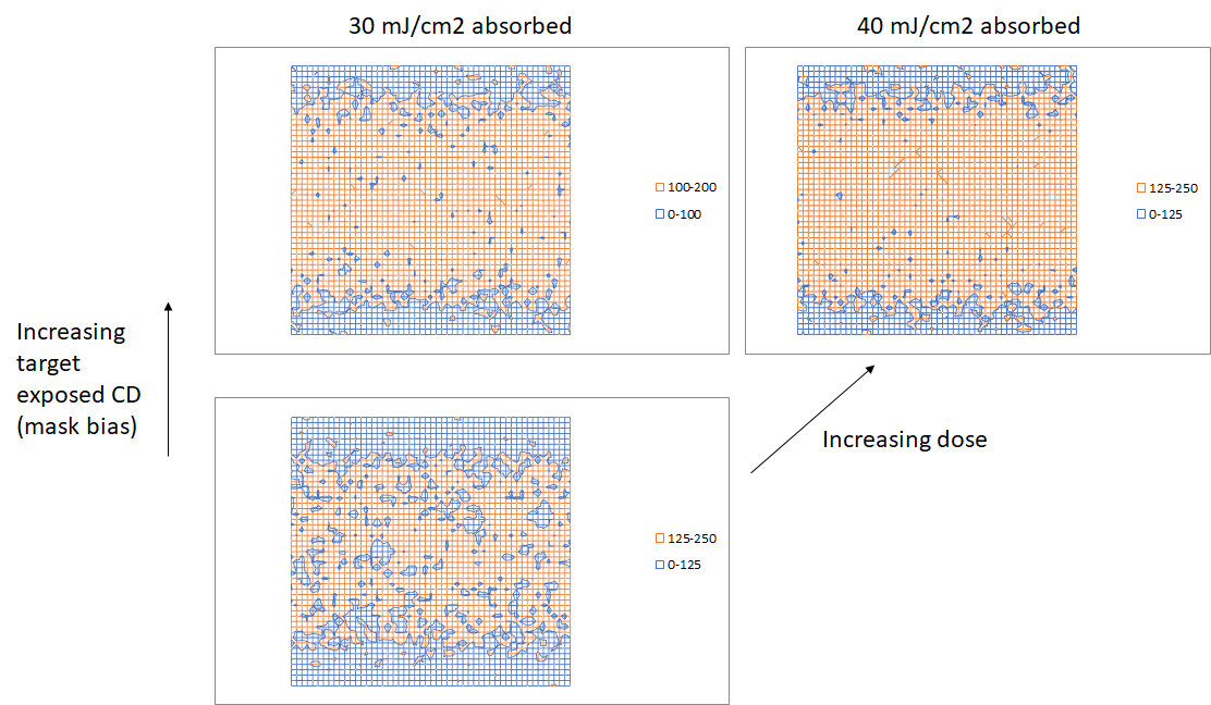
The simulation model combines three stages of random number generation: (1) photon absorption, (2) secondary electron yield, and (3) electron dose-dependent blur range. Unexposed stochastic defects are dominant at low doses where there are too few photons absorbed. Exposed stochastic defects are dominant at higher doses where the rare (e.g., probability ~ 1e-8) ultrahigh (>10 nm) blur promotes too much secondary electron exposure near the threshold value for printing.

Higher blur makes it easier for smaller stochastic dose variations to cross the printing threshold, enabling exposed or unexposed defects.
One consequence of both insufficient low photon absorption and dose-increased blur causing defects is the emergence of a floor or valley for stochastic defects, preventing them from being absent entirely.

At lower dose or exposed CD there tend to be unexposed defects, while at higher dose or exposed CD there tend to be exposed defects. This results in a floor or valley for stochastic defect occurrence.
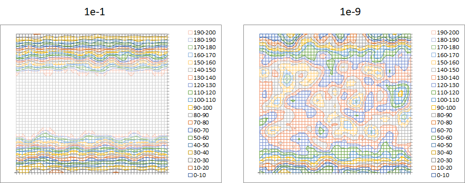
Another way to interpret the defect floor or valley is that the enlarged blur range at low enough probability increases the entropy significantly and damages the image across all possible printing thresholds.

With the much larger blur range at low enough probabilities (1e-9 in this example), there is significant entropy in the image and the image is damaged regardless of printing threshold. At more commonly observed probabilities (e.g., 1e-1), the image preserves its usual appearance. Note: the raw pixel images were smoothed for better visualization.
It is therefore very risky to not include dose-dependent secondary electron blur ranges in any model for EUV lithography image or defect formation.
References
[1] I. Bespalov, “Key Role of Very Low Energy Electrons in Tin-Based Molecular Resists for Extreme Ultraviolet Nanolithography,” ACS Appl. Mater. Interfaces 12, 9881 (2020).
[2] S. Grzeskowiak et al., “Measuring Secondary Electron Blur,” Proc. SPIE 10960, 1096007 (2019).
[3] D. Van Steenwinckel et al., “Lithographic Importance of Acid Diffusion in Chemically Amplified Resists,” Proc. SPIE 5753, 269 (2005).
[4] T. Brunner et al., “Impact of resist blur on MEF, OPC, and CD control,” Proc. SPIE 5377, 141 (2004).
[5] A. Narasimhan et al., “Studying secondary electron behavior in EUV resists using experimentation and modeling,” Proc. SPIE 942, 942208 (2015).
[6] M. Kotera et al., “Extreme Ultraviolet Lithography Simulation by Tracing Photoelectron Trajectories in Resist, Jpn. J. Appl. Phys. 47, 4944 (2008).
[7] M. Yoshii et al., “Influence of resist blur on resolution of hyper-NA immersion lithography beyond 45-nm half-pitch,” J. Micro/Nanolith. MEMS MOEMS 8, 013003 (2009).
[8] F. Chen, “EUV Stochastic Defects from Secondary Electron Blur Increasing With Dose,” https://www.youtube.com/watch?v=Q169SHHRvXE, 8/20/2023.
This article first appeared in LinkedIn Pulse: Modeling EUV Stochastic Defects With Secondary Electron Blur
Also Read:
Enhanced Stochastic Imaging in High-NA EUV Lithography
Application-Specific Lithography: Via Separation for 5nm and Beyond
Share this post via:


Solving the EDA tool fragmentation crisis