You are currently viewing SemiWiki as a guest which gives you limited access to the site. To view blog comments and experience other SemiWiki features you must be a registered member. Registration is fast, simple, and absolutely free so please,
join our community today!
Veriest is headquartered in Israel with engineering sites in Serbia & Hungary. The team has accumulated a wealth of experience through involvement in projects in the forefront of semiconductor technology.
Veriest maintains unrivaled quality standards in terms of both service and knowledge. With the ability to take on … Read More
In 2016 SemiWiki published a book “Prototypical: The Emergence of FPGA-Based Prototyping for SoC Design”. Today we are writing Prototypical II since a LOT of prototyping innovation has happened in the last four years, absolutely.
For example:
Quad 10M Prodigy™ Logic System extends the capacity leadership to simplify… Read More
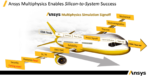
Innovative Designs Enabled by Ansys Semiconductor
I’m excited to announce that general registration is now open for the new Ansys IDEAS Digital Forum! IDEAS, hosted by Ansys Semiconductor, is a virtual gathering of top industry executives, thought leaders, and designers from some of the biggest IP, chip design, semiconductor… Read More
After spending a significant amount of my career in the IP library business it was an easy transition to Solido Design. I spent 10+ years traveling the world with CEO Amit Gupta working with the foundries and their top customers. In fact, the top 40 semiconductor companies use Solido. IP companies are also big Solido users including… Read More
Talk to the members of a digital design team and you will always find two types of users. One who likes using the GUI while working on his design and the other who is passionate about using scripts and the command line options. This is akin to the two camps of users who either love either good old Vi/Vim or the ever versatile Emacs editor.… Read More
Charlie Janac is president and CEO of Arteris IP where he is responsible for growing and establishing a strong global presence for the company that is pioneering the concept of NoC technology. Charlie’s career spans over 20 years and multiple industries including electronic design automation, semiconductor capital equipment,… Read More
Altair PBS Professional™ is the trusted leader in high-performance computing workload management. It efficiently schedules HPC workloads across all forms of computing infrastructure, and it scales easily to support systems of any size — from clusters to the largest supercomputers.
Scheduling for high-throughput workloads… Read More
The ARC Processor has a rich history. Originally named the Argonaut RISC Processor, it was designed for the Nintendo Game Systems in the 1990s. Argonaut Technologies Limited later became ARC International. My first intimate exposure to ARC was in 2009 when Virage Logic acquired ARC. A year later Virage was acquired by Synopsys… Read More
While Alchip is speeding its way down the TSMC process technology roadmap I am reminded how important services are to the semiconductor ecosystem. We can thank ASIC companies like Alchip for the heavy investment systems companies have made into semiconductors. We covered this in our book “Fabless: The Transformation of the Semiconductor… Read More
Anna has more than 25 years of expertise in managing complex R&D organizations and programs, giving birth to a number of innovative EDA technologies. She has pioneered the study and development of several generations of IC and package co-design environments and has held senior positions at leading semiconductor and EDA … Read More


Captain America: Can Elon Musk Save America’s Chip Manufacturing Industry?