You are currently viewing SemiWiki as a guest which gives you limited access to the site. To view blog comments and experience other SemiWiki features you must be a registered member. Registration is fast, simple, and absolutely free so please, join our community today!
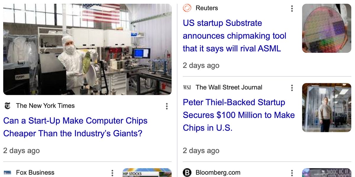
“Substrate” has been in the news for, allegedly, coming up with a way to make computer chips for much cheaper and at much higher quality than anyone else in the industry.
There’s just one problem: all signs indicate that the entire business is fake.
- The founder is known con-artist involved in such other things as solving nuclear fusion and stealing $2.5M in a Kickstarter scam.
- The cofounder is the founder’s brother and has literally zero documented professional or academic experience.
- The company’s job postings are nonsensical and AI-generated
- The company is unwilling to evidence any of its (extremely extraordinary) claims, which have been made on a timescale that makes no sense in the context of the semiconductor industry
- The company’s research facility is, based on photographs that they’ve published, at least two orders of magnitude smaller than what would be necessary.
Ebeam lithography and multi-beam has been in existence for years (maybe decades) but they are used to make masks not chips.
If the requirement is to make one chip per week per machine, yeah, certainly possible (may even improves to 2 chips a week, lol). But you better be prepared to build fabs the size of superdome or bigger.
Or unless he might have figured out how to flatten a chip design to just one single layer, without the need of muiltiple layers needing mask and exposure.
It's hard to tell -- there is entanglement though of some kind, per Semianalysis:
" Note we have worked with Substrate since as far back as 2022, but the technical analysis here was by team members who did not have access to that NDA information."
Substrate X-Ray Lithography, a New American Foundry, $10k Logic Wafers
newsletter.semianalysis.com
... Further down, this article does point out challenges:
Naysayers will point out a million reasons why this is improbable, difficult, etc. - and they are mostly correct. There is a big difference between lab-scale and industrialized, high-volume tools. Substrate itself realizes this and agrees they are in for a lot of development and scaling pain.
... and their summary doesn't read like they're part of this:
Most of this report is based on the promise of Substrate. A novel demo tool with these imaging capabilities built in 2 years is impressive. But there is a lot more to prove before they disrupt the chipmaking industry. We're hopeful for success but skeptical given how many questions there are. We’re looking forward to a few milestones that will silence the skeptics (both internal and external):
It's hard to tell -- there is entanglement though of some kind, per Semianalysis:
" Note we have worked with Substrate since as far back as 2022, but the technical analysis here was by team members who did not have access to that NDA information."
SemiAnalysis is an LLC registered to Dylan Patel, who also does not have academic or professional semiconductor experience so what exactly was Substrate paying him for as far back as 2022?
This is pretty strong language from FCR. Someone may have an axe to grind here:
- The founder is known con-artist involved in such other things as solving nuclear fusion and stealing $2.5M in a Kickstarter scam.
- The cofounder is the founder’s brother and has literally zero documented professional or academic experience.
Here is what I found on FCR which, in my opinion, is sketchy to say the least:
Fox Chapel Research (FCR) appears to be an independent, anonymously-run research newsletter published on Substack, focusing on deep-dive investigations into semiconductor- and technology-industry companies.
I have no idea what Folsom St Labs is or does but it is seemingly related to both James Proud and his brother, the founders of Substrate. Apparently they were inventing biotechnology and nanotechnology while solving nuclear fusion and inventing a better-than-ASML-scanner lithography method.
This really does read like a made for Netflix series.
Lol agreed Substrate sounds sketchy. It's just not clear yet what Dylan's level of involvement is; though it is leaning he may have been used to ... Help fleece, er, get investors.
(Disclosure - I have a negative opinion of Dylan, but am trying to stay unbiased here in my wording though.)
Lol agreed Substrate sounds sketchy. It's just not clear yet what Dylan's level of involvement is; though it is leaning he may have been used to ... Help fleece, er, get investors.
(Disclosure - I have a negative opinion of Dylan, but am trying to stay unbiased here in my wording though.)
it is important to note that Substrate has no intention of selling them to third parties such as Intel or TSMC. Instead, Substrate plans to build its own fabs in the U.S.
Dylan may have a good team now but he was alone for the first few years and he was selling snake oil (my opinion). We worked with him a bit in 2021/2022 but his lack of experience showed through so we did not continue. The straw that broke the camels back per say was when he called TSMC a drug dealer. He apologized but there was no going back after that.
SemiAnalysis: "TSMC, The Drug Dealer, Is Trying To Make An Addicted Junkie Out Of Intel – Wafer Supply Agreement Insights For AMD, Apple, Broadcom, Intel, MediaTek, Nvidia, and Qualcomm"
The Substrate story is becoming even more interesting. Below is an article from one of the Substrate's investors, a venture capital firm called Long Journey:
"And you know what? That's exactly why it might work. Because James Proud has something ASML's executives don't have, something TSMC's board doesn't have: the bone-deep knowledge of what it's like to fail, to rebuild, and to come back with a chip on your shoulder the size of Texas.
He's not trying to build a better mousetrap. He's trying to build the mousetrap factory that saves Western civilization. The stakes couldn't be higher, and the founder couldn't be more battle-tested."
Talking about the tattoo:
"Well, ultimately it's a symbol. A symbol of belief in James Proud and his team. He was forged in fire and came out unbroken."
He got his undergrad buisiness degree from the University of Georgia (between 2015-2020) and then started SemiAnalysis in 2020. He is a self taught expert who bootstrapped himself into an expert widely sought after his expertise.
"Reimagining Chipmaking
We first invested in Substrate’s seed round more than three years ago, confident in founder James Proud’s trifecta of strengths: expertise in global hardware and supply chains, a first-principles founder mindset, and a deep passion for solving complex national security challenges once thought unsolvable.
James founded Substrate with several core convictions. He saw that the cost of semiconductor fabrication was rising rapidly and would continue to increase without a new technology paradigm. He also recognized that the U.S. was heavily reliant on a small number of external sources, creating significant geopolitical and supply chain risks. In his view, the only way to restore U.S. leadership in advanced semiconductor production was to create a completely new kind of vertically integrated foundry from the ground up.
It took nearly two decades and billions of dollars for traditional EUV lithography, the current manufacturing standard, to reach maturity. In comparison, Substrate has already successfully demonstrated its technological approach in a fraction of the time and cost.
As seen in many industries transformed by technology, real breakthroughs often come from teams outside the established players who bring a first-principles approach to long-standing problems. Substrate’s world-class team of multidisciplinary experts includes scientists and engineers from leading U.S. national research labs, including co-creators of EUV lithography, as well as top talent from companies such as AMD, Apple, Applied Materials, Qualcomm, and TSMC. Their ability to start from a clean slate allowed them to pursue a fundamentally different path to advanced lithography, enabling chip production at leading-edge nodes while significantly reducing cost and complexity."
I think to realize Substrate's goal (which by the way seems to encompass ASML and TSMC's market reach), you need at minimum:
1. Unlimited investment funding,
2. Guaranteed customers who will buy your wafers at high prices even before you can come close to what your competitors can do,
3. Engineers who are inspired and fired up by the vision and thinks they can win.
Ironically the Chinese semi industry had only (1) going for them before the US cut them off. Now they have all 3.
>But here's what most people don't understand about failure at this scale: it teaches you things success never could. Every burned bridge becomes a lesson in structural engineering. Every wrong turn becomes a data point. Every dollar lost becomes tuition for the most expensive MBA program in the world, the one where the classroom is the market and the professors are your failures.
Source: https://www.longjourney.vc/news/cyans-substrate-tattoo
But, Billionaire Peter Thiel: ‘Failure is massively overrated’
PayPal co-founder and billionaire investor Peter Thiel has a different opinion. “I think failure is massively overrated,” he tells author Tim Ferriss in ″Tools of Titans.″ “I think people actually do not learn very much from failure.”
" Note we have worked with Substrate since as far back as 2022, but the technical analysis here was by team members who did not have access to that NDA information."
From the Semianalysis article How to Kill 2 Monopolies with 1 Tool:
There are four authors listed: Dylan Patel, Jeff Koch, Gerald Wong, and Andrew Wagner.
“Evidence so far is scarce, so we repeat these claims with some healthy skepticism. But we should also note, external contacts and 3rd party reports are all telling us the same story: the litho tool is legit. Note we have worked with Substrate since as far back as 2022, but the technical analysis here was by team members who did not have access to that NDA information.”
In my opinion, having a public report co-authored by a group of people mixed with those who may or may not have signed an NDA with Substrate creates a problematic situation. It potentially undermines the credibility of the analysis and the authors.
Worse, if the report later turns out to include inaccuracies, omissions, or exaggerated claims, could Dylan argue that the NDA prevented him from providing full details or corrections? That explanation would not be convincing to most readers.
If Substrate wanted Mr. Patel to publicly write about the company’s breakthrough technology, then Mr. Patel should not signed an NDA in the first place. Or, if he is bound by an NDA, then he should refrain from publishing analysis that he cannot thoroughly confirm or deny publicly.
After all, it would be strange if a company CEO or even the US President invited a journalist for an interview but simultaneously required the journalist to sign an NDA that restricts what he/she can report.

 substack.com
")