You are currently viewing SemiWiki as a guest which gives you limited access to the site. To view blog comments and experience other SemiWiki features you must be a registered member. Registration is fast, simple, and absolutely free so please,
join our community today!
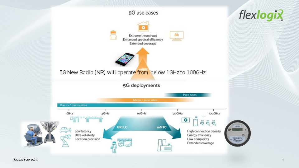
The demands of 5G requires new designs to not only save power but also increase performance and by moving to advance power-saving nodes and by using eFPGAs will help to achieve these goals. This paper will introduce 5G and O-RAN, the complexity of these systems, and how flexibility could be beneficial. Then we will dive into how eFPGA… Read More
One of the recent live events I attended was the 2022 GSA Silicon Leadership Summit on May 12th at the Santa Clara Convention Center (my favorite location). This was the first GSA live event in two years so it was a must attend gathering. This event targets semiconductor ecosystem executives (200+ people attended) so there were many… Read More
The live events I have attended thus far this year have been very good. As much as I liked the virtual events, attending in the comfort of my home or sailboat, it is great to be live and networking inside the semiconductor ecosystem, absolutely.
Ansys has been a great supporter of the Design Automation Conference but this year they … Read More
Vaysh Kewada is cofounder and CEO at Salience Labs, a company developing an ultra high-speed multi-chip processor that packages a photonics chip together with standard electronics to enable exascale AI. Salience is funded by Oxford Sciences Enterprise, Cambridge Innovation Capital, Arm-backed Deeptech Labs, former Dialog… Read More
With the TSMC Technical Symposium coming next month there is quite a bit of excitement inside the fabless semiconductor ecosystem. Not only will TSMC give an update on N3, we should also hear details of the upcoming N2 process.
Hopefully TSMC will again share the number of tape-outs confirmed for their latest process node. Given… Read More
The tremendous increase in global data traffic over the past decade shows no sign of abating. Indeed, the applications for all facets of data communications are expanding, from 5G (and soon, 6G) wireless communications to metropolitan area networks serving autonomous vehicles to broader deployment of machine learning algorithms. … Read More
Chuck Gershman CEO is the co-founder Owl Autonomous Imaging, Inc. Chuck is a Drexel University College of Engineering inductee into the Alumni Circle of Distinction, the highest honor bestowed upon alumni. He has been honored as a finalist for CMP publications (EE Times) prestigious ACE award as High Technology Executive of… Read More
Earlier this year semiconductor oracle Malcom Penn did his 2022 forecast which I covered here: Are We Headed for a Semiconductor Crash? The big difference with this update is the black economic clouds that are looming which may again highlight Malcolm’s forecasting prowess. I spent an hour with Malcolm and company on his Zoom cast… Read More
Proper clock functionality and performance are essential for SoC operation. Static timing analysis (STA) tools have served well for verifying clocks, yet with new advanced process nodes, lower operating voltages, higher clock speeds and higher reliability requirements, STA tools alone can’t perform the kinds of analysis… Read More
Dr Ali El Kaafarani is the founder and CEO of PQShield, a British cybersecurity startup specialising in quantum-secure solutions. A University of Oxford spin-out, PQShield is pioneering the commercial roll-out of a new generation of cryptography that’s fit for the quantum challenge, yet integrates with companies’ legacy
…
Read More

















SEMICON West’s Autonomous Fab Vision Needs a Decision-Escalation Design