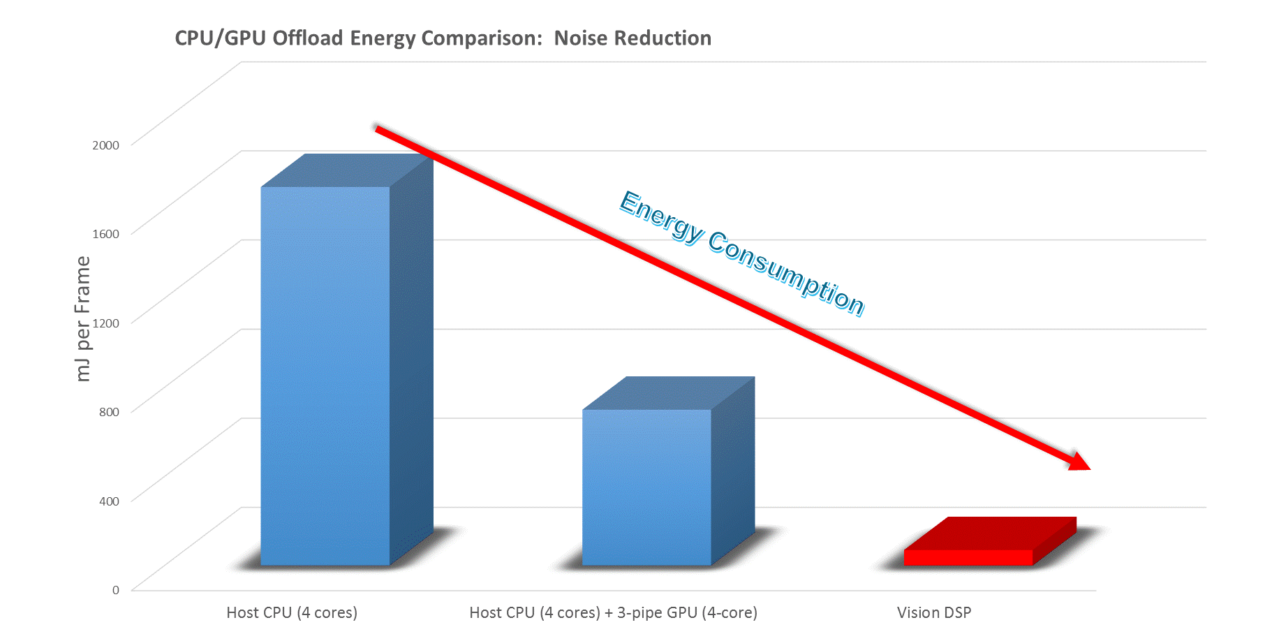
You may not know Tensilica DSP IP core, but you probably use Tensilica DSP powered systems in your day to day life. Every year, over 2 billion DSP cores equip IC in thousands of designs supporting IoT, Mobile Phones, Storage/SSD, Networking, Video, Security, Cameras… and more. Why DSP processing, the foundation of all Tensilica processors, is getting such high adoption? Just because DSP processing is more energy and area efficient than CPU or even CPU/GPU processing. If you compare the energy dissipated to process image (in mJoule per frame) when offloading to Host CPU (4 cores), Host CPU (4-cores) + 3-pipe GPU (4-cores) or to a Vision P5 DSP like Tensilica 4[SUP]th[/SUP] generation IP core you notice 30X reduction factor.

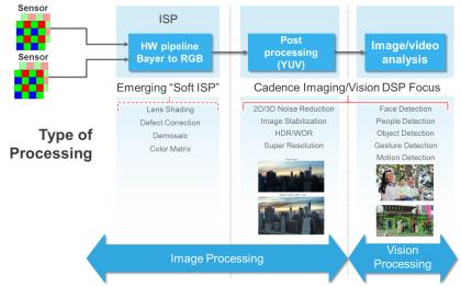
Imaging/Vision processing is required in more application every day, like Mobile phone when processing the raw image from the camera, automotive to support the multiples applications linked with Automotive Driver Assistance Systems (ADAS), 4K Ultra-HD or IoT. That why the 4[SUP]th[/SUP] generation of DSP from Tensilica is labeled “Vision P5”. Before looking at the DSP architecture, let’s clarify a point: this DSP is both an Image Signal Processor (ISP) and a Vision Processing Unit (VPU). Directly interfacing with sensors, ISP used to be implemented in hardwired logic (RTL), but the trend is to move to “Soft ISP”. If we take the example of face detection, moving to soft ISP allows dividing by 5X energy consumption. Cadence Imaging/Vision DSP focus on Image post processing and on Image/Video analysis. The slide below helps understanding this focus. Post processing includes 2D/3D noise reduction, image stabilization, Super Resolution, etc. when Image/Video analysis (face detection, people detection and more) is part of Vision Processing.

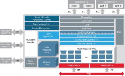
Cadence Vision P5 DSP core is a deeply pipelined design running up to 1.1 GHz (on 16nm FF technology), being low power thanks to massive clock gating implementation. The core supports 256 ALU ops/cycle due to the vector extensions based architecture: 4 vectors ops per cycle, each being 64-way SIMD. Vector extensions data can be 8-b, 16-b or 32-b. To support vision-based ADAS, drones, and augmented reality, the designer will have to implement an (optional) Vector Floating Point Unit (VFPU). This VFPU can deliver 32 GFLOPS per second for a core running at 1 GHz. This core supports industry widest 1024-bit memory interface and the memory system performance is greatly improved, thanks to scatter/gather data registers. Up to 16X faster random memory access can be achieved for non-uniform access algorithms like image warping, edge tracing, non-rectilinear patch access… Finally, like the others Tensilica DSP IP core, the Vision P5 DSP core allows customers to add their own instruction set.

To support massive computing needs, multiple Vision P5 DSP cores can be implemented. Multi-core support shared memory and message-passing architectures. A five cores implementation can deliver up to 1 Tera-ops (1,000,000,000,000 operations per second !) but which is really amazing is the footprint : 2 sq mm in 16nm FF technology.
Imaging and vision processing is a very fast moving market, OEM are constantly changing optics, sensors, and new algorithms have to be developed to support emerging applications like face detection, face recognition. ADAS is becoming a reality and in the near future we can expect the car manufacturers and their suppliers to imagine many new applications and create new algorithms. They just need highly programmable and flexible engine, scalable thanks to multi-core capability. The 4th generation of Tensilica DSP, the Vision P5, has been developed by Cadence to support such applications.
By Eric Esteve from IPNEST
Share this post via:


Comments
There are no comments yet.
You must register or log in to view/post comments.