
- This event has passed.
Webinar: Design Exploration of RF GaN Amplifier, 3D Packaging, and Thermal Analysis
February 7 @ 12:00 PM - 1:00 PM
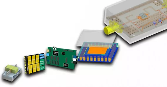
Join us for this webinar on RF GaN amplifier design using electromagnetic/thermal 3D solvers. We will discuss the step-by-step process of building a GaN amplifier, beginning with the transistor model in the circuit simulator. The webinar will outline the steps required to convert this to a physical layout for electromagnetic simulation and verification while integrating packaging and thermal effects co-simulation to analyze a complete packaged system. Discover how this comprehensive approach yields innovative solutions, important design insights, and their potential impact on packaged performance.
Time:
February 7, 2024
9 AM EST / 3 PM CET / 7:30 PM IST
Venue:
Digital
What You Will Learn
- Design and layout of a typical GaN amplifier using circuit
and 3D EM tools - Incorporation of 3D component models (connectors, packages etc) for complete system analysis
- Co-simulation of packaged devices with thermal solvers
Who Should Attend
- Electromagnetic and circuit design engineers: Delve into the co-
simulation nuances between circuit models and full 3D designs - System engineers: Develop an understanding of the packaged PA design and tradeoffs
- Professionals in wireless communication: Gain comprehensive
insights into the modern circuit/package co-simulation
workflows
Speaker
David Edgar, Senior Manager Applications Engineer
Share this post via:


Application-Specific Lithography: Sense Amplifier and Sub-Wordline Driver Metal Patterning in DRAM