
My first IC design back in 1978 was a DRAM and it ran on 12V, 5V and -5V, but then my second DRAM was using only a 5V supply. Today we see SOCs running under a 1V supply voltage, but there is a totally different market for power devices that are at the other end of the voltage spectrum and they handle switching ranges from 12V – 250V. To learn more about power devices and how the process and device modeling is done, I read a Silvaco publication entitled Advanced Process and Device 3D TCAD Simulation of Split-Gate Trench UMOSFET.
For vertical discrete power MOSFETs there are two important specifications that engineers look at:
- Breakdown voltage (BV)
- Specific on-state resistance (RSP)
A couple of approaches have been used for power devices: Trench MOSFETs, RSO MOSFETs. The winning approach has been the Split-Gate RSO MOSFETs because of their low channel resistance, plus ultra-low drift region resistance with a smaller Cgd (gate-to-drain capacitance), improving switching speeds.
Process engineers use 3D TCAD tools to model power devices and optimize them by looking at the predicted values of:
- Capacitance-Voltage (C-V)
- Current-Voltage (I-V)
- Breakdown Voltage (BV)
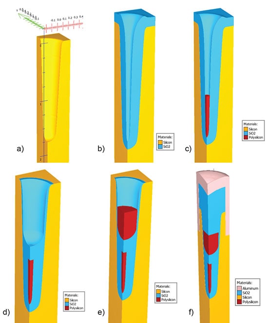
Silvaco provides Victory Process and Victory Device simulators to do this modeling of power devices. So let’s start with a 3D process simulation of a Split-Gate UMOSFET, where Victory Process is used to build the device structure. Several simulated process steps are shown below:
a) Formation of a deep trench with rounded bottom, both dry and wet etch steps
b) Shield oxide growth
c) Shield poly deposition
d) Inter-poly oxide deposition and etch back
e) Gate poly deposition and etch back
f) Core contact etching and deposition of the contact plug
A 3D numerical mesh is the next step using the Victory Mesh tool, and a 3D Delaunay mesh was generated to accurately resolve the 3D geometrical features. Here’s the result of meshing:
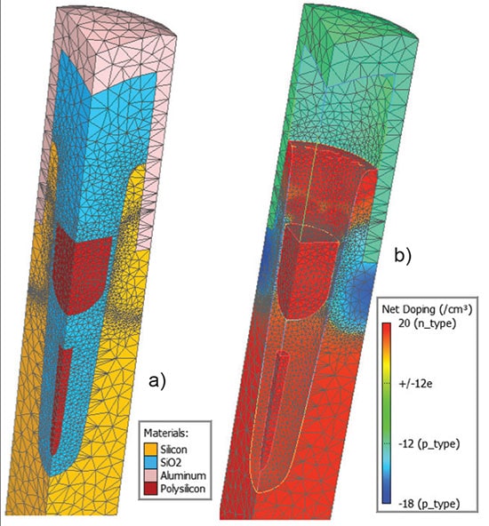
3D device simulations are then run with the Victory Device simulator, and this is quite powerful because it can model 3D unstructured tetrahedral meshes for any device shape. To run Victor Device simulations you have several actions:
- Specify the materials, models and simulation values
- Simulate steady-state Id-Vg, gm-Vg, Id-Vd and BV
- Small-signal (AC) capacitance-voltage (C-V) plot
- Device switching plots
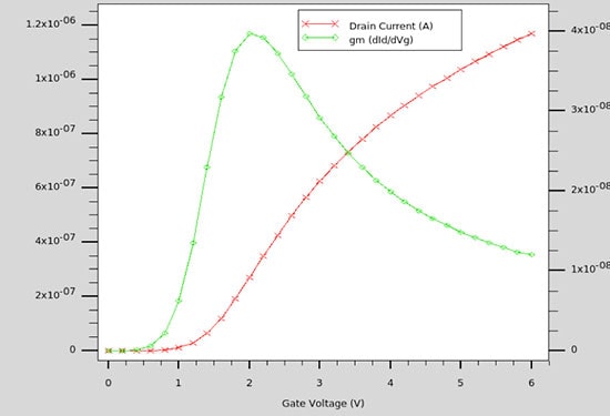
An initial solution is computed, then Id-Vg curves are produced for each Vds voltage, then transconductance gm-Vg are computed as shown below:
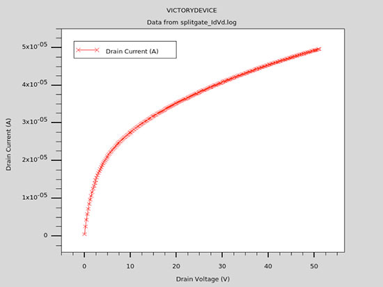
Here’s the plot of Id-Vd at a select Vgs bias voltage:
A plot of Breakdown I-V is shown where the gate bias Vg = 0V:
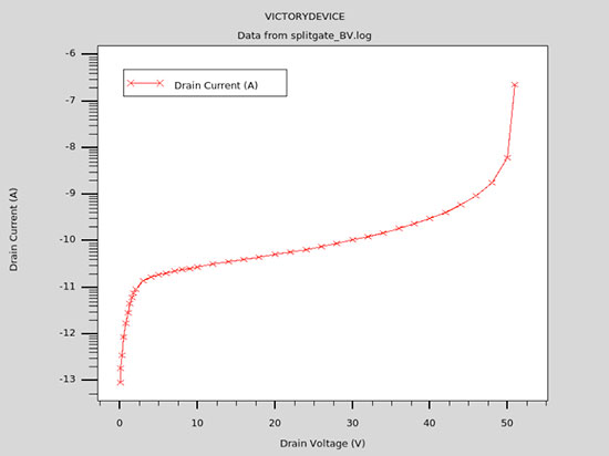
Each of these I-V curves was generated by the TonyPlot tool.
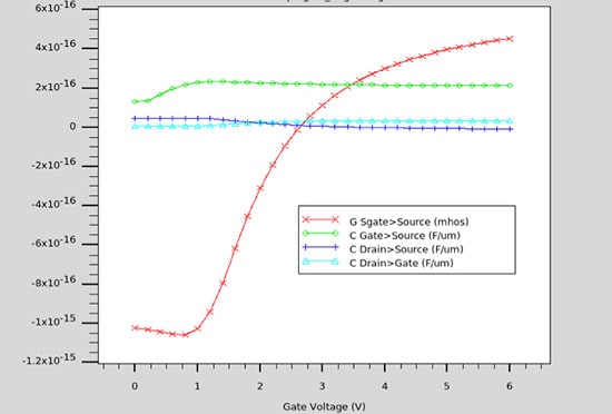
C-V plots are simulated with Victory Device, and here’s the small-signal (AC) results showing intrinsic capacitances:
Summary
Process engineers equipped with the proper modeling and simulation tools can now predict the behavior of power devices like Split-Gate Resurf Stepped Oxide (SG-RSO) MOSFET. Instead of running lots of silicon, measuring, tweaking and repeating, engineers can accurately model and optimize virtually, saving lots of time and money. Read the complete article online.
Related Blogs
- Silvaco Talks Atoms to Systems – Where to Next?
- Silvaco Samsung and Excitement at 56thDAC
- WEBINAR: Nanometer Library Characterization Challenges and Solutions
- Silvaco on Simulation of Reliability and NBTI Aging in MOS Microelectronics
- Where Circuit Simulation Model Files Come From


Has ASML Reached the Great Wall of China