Bronco Webinar 800x100 1

UVM: Lowering the barrier to IP reuse

UVM: Lowering the barrier to IP reuse
by Don Dingee on 02-06-2013 at 2:00 am

One of my acquaintances at Intel must have some of the same viewing habits I do, based on a recent Tweet he sent. He was probably watching “The Men Who Built America” on the History Channel and thinking as I have a lot recently about how the captains of industry managed to drive ideas to monopolies in the late 1800s and early 1900s.

Difference between 1800’s & today is that barriers to entry r so low & marketplace is so varied that monopolists have very narrow domains.

The comment on technological barriers being lowered is true, especially in a new semiconductor industry that relies more and more on merchant foundries and commercial IP, now the building blocks of choice for most teams. Variation in the market is also a truism, and it is forcing former deathly rivals to cooperate so that all may prosper – a distinct shift in thinking from the winner-take-all thinking that dominated so much of the Industrial Age.

In an EDA industry marked by at least three distinct approaches, the shift in the landscape is driven by a huge problem: IP has only been reusable under carefully controlled conditions, usually meaning adoption of a particular tool chain and verification methodology. Paradoxically, as more IP has been developed, the problem has worsened. Not only does new IP require design and test, but steps are being retraced to reengineer and integrate existing IP into new environments. This mix eventually becomes overwhelming, if not for design resources then certainly for test resources.

The genesis of Universal Verification Methodology (UVM) fascinated a lot of people, wondering why Cadence, Mentor, and Synopsys would cooperate, or even be seen in the same photo. Unifying the disparate approaches to IP verification lowers a major barrier to IP integration and reuse, and UVM provides a better and faster way to test using coverage-driven verification.

More people are getting interested in UVM and SystemVerilog, including participants here at SemiWiki – here are a couple samples of recent forum contributions:

Evolution of the test bench – part 2
SVA : System Verilog Assertion is for Designer too!!

As with any new standard, it takes time for people to understand and embrace the technology. Both the hardware IP designer and the test/verification engineer should take note. The definitive source document is the UVM 1.1 User Guide, free for open download at Accellera.

A new learning resource has debuted this week. Aldec has launched their Fast Track ONLINE training portal, with a series of modules planned on UVM. These self-paced modules give practical examples of concepts related to SystemVerilog, transaction level modeling (TLM), and more on the standard and how to implement it.

Registration is simple, and Fast Track training modules are free.

Creating and leveraging truly reusable IP is one of the keys to getting more designs done, tested, and launched. Success in reusing IP – hardware, software, design, test, everything that goes into the final integrated product – frees up resources for innovative breakthroughs and differentiation of platforms. UVM is a positive change for the EDA industry, and should be a major help for designers willing to embrace it.


Could “Less than Moore” be better to support Mobile segment explosion?

Could “Less than Moore” be better to support Mobile segment explosion?
by Eric Esteve on 02-05-2013 at 4:52 am

If you take a look at the explosion of the Mobile segment, linked with the fantastic world-wide adoption of smartphone and media tablet, you clearly see that the SC industry evolution during –at least- the next five years will be intimately correlated with the mobile segments. Not really a surprise, but the question I would like to raise is: “will this explosion of SC revenue in mobile segment will only be supported be applying Moore’ law (race for integration, more and more functionalities in a single chip targeting the most advanced technology nodes), or could we imagine that some subsequent mobile sub-segment could be served by less integrated solution, offering much faster TTM and finally better business model and more profit?”

At first, let’s identify today’s market drivers, compared with these of the early 2000’s. At that time, the PC segment was still the largest, we were living in a monopolistic situation and Intel was benefiting from Moore’s law, technology node after technology node. If you schematize, the law says that you can choose between dividing the price by 2 (for the same complexity) or doubling the complexity (for the same price), and in both cases increase the frequency. Intel clearly decided to increase the complexity, keep the same die size… and certainly not decrease the price! TTM was not really an issue for two reasons: Intel was (and still is) the technology leader, always the first to support the most advanced node, and the company was in a quasi-monopolistic situation.

The explosion of mobile has changed the deal: performance is still a key factor, but the most important is power consumption (say MIPS per Watt). Price has becoming a much more important factor, even if performance is still key, on such a competitive market, with more than 10 companies addressing the Application Processor market. And TTM is also becoming a key factor on such a market.
To summarize, we move from a PC market where (Performance, somewhat TTM) are the key factors to a Mobile market where (MIPS per Watt, Price, TTM) are keys. Unfortunately, I don’t think that following Moore’s law in a straight way can efficiently address these three parameters…

  • Leakage currentis becoming such an important, as highlighted in this article from Daniel Payne, that going forward will help increasing the CPU/Logic performance, but may decrease at the end the power efficiency (MIPS per Watt)! This has forced design teams to use power management techniques, but the induced complexity has a great impact on IC development and validation lead-time…
  • Price: we talk about IC Average Selling Price (ASP), the chip maker think in term of “cost”, at first, then ASP when they sell the IC. There are two main factors affecting this cost: IC development cost (Design resources, EDA, IP budget, Masks, Validation…) and chip fabrication cost in production (Wafer, Test, Packaging). If you target an IC ASP in the $10/20 range, like for example an Application Processor for smartphone, you quickly realize that, if your development cost is in the $80 million range (for a chip in 20nm), you must sell… quite a lot of chips! More likely, the break-even point is around 40 or 50 million chip sold!
  • Time-To-Market(TTM): once again, we are discovering that, for each new technology node, the time between the design start and the release to production (RTP, when you start to get return on your investment) is longer and longer. It would take a complete article to list all the reasons, going from Engineering gap to longer validation lead-time, passing by wafer fab increased lead-time, but you can trust me: strictly following Moore’s law directly induces a longer overall lead-time to RTP!

Does that mean that Qualcomm, for example, is wrong when proposing the above 3 step road-map, ending with a single chip solution? Certainly not… but they are Qualcomm, the emerging leader (and for long time in my opinion) in the mobile segment, offering the best technical solution, with a TTM advantage. But, if you remember, more than two Billion systems will ship in the mobile segment by 2016, which means about 20 billion IC… We can guess that Qualcomm will NOT serve all the mobile sub-segments, thanks for the competition able to enjoy some good piece of business! This article is addressing Qualcomm (and Samsung or even Apple) followers: “Less than Moore” could be a good strategy too! I realize that it will take another post to describe which could be the possible strategies linked to “Less than Moore”, so, please be patient, I will release this in a later article…

From Eric Esteve from IPNEST


Sanjiv Kaul is New CEO of Calypto

Sanjiv Kaul is New CEO of Calypto
by Paul McLellan on 02-04-2013 at 11:15 am

Calypto announced that Sanjiv Kaul is the new CEO. I first met Sanjiv many years ago when he was still at Synopsys when I interviewed for a position there around the time I transitioned out of Compass and went back to the parent company VLSI. I forget what the position was. Then about three or four years ago when I did some work for Oasys he was on the board there and was their executive chairman and helping them with marketing part time. Funnily enough, Oasys got a new CEO too just before the end of last year.

Sanjiv was senior VP and GM for physical compiler when he was at Synopsys. Prior to that he was the marketing director for the launches of PrimeTime and Formality. Since then he has been involved in many startups, not all EDA, as advisor, board-member or in operational roles.

Apparently this has been very closely held. Calypto’s PR agency only found out today and the Calypto website still hasn’t been updated yet. UPDATE: now it has been updated.

And here he is again, looking rather less CEO-like, along with Paul van Besouw and Joe Costello from Oasys’s DAC video four years ago.

Press release is here.

Also Read:

Atrenta CEO on RTL Signoff

CEO Interview: Jason Xing of ICScape Inc.

CEO Interview: Jens Andersen of Invarian


Software Driven Power Analysis

Software Driven Power Analysis
by Paul McLellan on 02-03-2013 at 8:15 pm

Power is a fundamentally hard problem. When you have finished the design, you have accurate power numbers but can’t do anything about them. At the RTL level you have some power information but it is often too late to make major architectural changes (add an offload audio-processor, for example). Early in the design, making changes is easy but you often lack accurate data to use to guide what changes make sense.

In many systems, power depends on what the SoC is doing and, in turn, that depends on the software. For example, a cell-phone obviously consumes different amounts of power when you are making a call from when it is just sitting in your pocket. In fact the power changes dramatically depending on whether you are talking (lots of data to transmit) versus listening (the transmitter, a huge power hog, is mostly idle). What the system is doing depends largely on what the software on the phone has enabled and disabled.

Assuming you have a virtual platform, and there are all sorts of reasons why you should that have been covered in earlier blogs, then you can use it to do power analysis. The reality in many SoC designs is that the power consumption depends on the contents of a comparatively small number of registers that enable or disable various functions, maybe disable their clocks, maybe power them down completely.

To do architectural power analysis proceeds in three steps. Firstly, identify the critical registers that alter the system behavior in ways that have a big impact on power. For example, going back to the cellphone there are probably registers that enable and disable the transmit and receive logic for the radio. If it is a multi-mode phone (GSM and CDMA) for sure there are registers that disable the logic associated with the unused standard. There may be registers that change the clock frequency of DSPs or control processors.

Second, having identified the registers, for each setting of the registers, the blocks concerned need to be analyzed for power using traditional EDA power analysis, probably at the RTL level unless more detailed information is available. The more “typical” the vectors you can get your hands on the better. Functional verification vectors are usually not very good for this since they are trying to exercise as many corner cases as possible, which, by definition, don’t happen very often.

So now you have a table of registers, and for each setting of those registers you have average power numbers. Next, instrument the virtual platform with callbacks. Each time the value of one of those registers changes then that needs to call back the virtual platform infrastructure and ultimately be logged along with the time or the clock-cycle.

Now you have a fully instrumented system. How do you exercise it? You run the software load. There are probably various software scenarios (boot, standby, listening to mp3, making a call, sending a text, surfing the net, using GPS and so on). You can run as many of these as is appropriate. You will end up with a logfile that shows when every register that has major effect on power changes. It is straightforward to work out what the average power for each block was and for how long, and then to add them up to get a total power number for that scenario. Obviously the total power for a system like a cellphone depends on what assumptions you make about how it is used. A teenager listening to mp3s all day and sending lots of text messages will have very different power consumption (aka battery life) from a salesman who practically lives on the phone making calls.

This doesn’t work for every SoC. In particular, if the power is very dependent on the data more than the mode the chip is in, then it is very important to have realistic data streams. Many SoCs are not like that though. A cellphone’s depends much more on whether you are speaking and hardly at all on what you say.

Download the Carbon whitepaper here.


Help, my IP has fallen and can’t get up

Help, my IP has fallen and can’t get up
by Don Dingee on 02-03-2013 at 8:10 pm

We’ve been talking about the different technologies for FPGA-based SoC prototyping a lot here in SemiWiki. On the surface, the recent stories all start off pretty much the same: big box, Xilinx Virtex-7, wanna go fast and see more of what’s going on in the design. This is not another one of those stories. I recently sat down with Mick Posner of Synopsys, who led off with this idea:
Continue reading “Help, my IP has fallen and can’t get up”


A Brief History of ClioSoft

A Brief History of ClioSoft
by Daniel Payne on 02-03-2013 at 8:05 pm

In the 1990s, software developers were established users of software configuration management (SCM) tools such as open source RCS/CVS or of commercial systems such as Clearcase. Hardware designers, however, managed design data in ad hoc home-grown ways. ClioSoft’s founder, Srinath Anantharaman, recognized that hardware development could benefit from some of the same techniques and methods as software development., Hardware design flows had some unique requirements not met by SCM tools and hardware designers were not as comfortable with Unix command line tools. Anantharaman wanted to fill this gap by creating a hardware configuration management (HCM) system that would help streamline hardware design teams just as SCM tools had done for software teams.

ClioSoft was launched in 1997, as a self-funded company, with the SOS (Save Our Software) design collaboration platform as its first product to help manage front end RTL flows. With the commercial deployment of the tool, ClioSoft soon realized that the greater need was to manage design data from analog/mixed-signal designs where Cadence Virtuoso® was the dominant flow. Designs were created using graphical tools like schematic or layout editors that produced large collections of binary files. Designers worked at the abstraction levels of libraries, cells, and views and were not familiar with the physical files created by the design tools. It would have been really difficult to use a file-based management method to manage Cadence Virtuoso data. ClioSoft joined the Cadence Connections™ program in 1998 and proceeded to work closely with Cadence to solve this problem. The result was a new product, SOS viaDFII, that seamlessly integrated the version control and design management features of SOS with the Cadence Virtuoso flow, allowing users of the Cadence Library Manager to manage revisions of schematics and layouts without worrying about the physical files.

Over time, the exponential increase in design complexity and shrinking market windows led to larger design teams. With increased globalization, design teams started getting distributed, recruiting the best talent wherever it was available. These dual forces increased the need for design management and efficient collaboration. To meet the new challenges, ClioSoft introduced the cache server in 2002. A cache server could be run at the remote sites to automatically cache the latest file revisions and serve these files to the users at the remote sites without having to get the data from the primary site. This made working at remote sites almost as efficient as working at the primary site and gave every engineer real time access to changes to design data without the requirement for a very high bandwidth connection.

As design team and design sizes grew, additional burdens were put on the already-stretched IT resources and staff at customer sites. File servers would run out of disk space and backups would never end. ClioSoft realized that much of the design data was being duplicated, since each engineer had entire copies of the design libraries in his or her workspace even though only a small portion of the design was being modified. Clearly there should be a way to avoid this duplication without taking away control of the workspace from the designer. ClioSoft solved this problem by introducing the capability to create workspaces with symbolic links into the cached revisions that already existed in the cache. Workspaces were now a lot smaller because most of the files were symbolic links to a file in the cache except for the few files the user was editing. ClioSoft cache server was now able to track how many users were using each revision of each file. It kept all revisions being used and automatically purged all unused revisions. The smart cache allowed optimum use of disk while still giving each user complete isolation and control of his or her workspace. This was widely adopted by design teams and now over 90% of design teams using SOS in the Virtuoso flow use workspaces with links to cache. This feature was a clear differentiator for ClioSoft as SCM systems created to manage relatively small text files did not support such optimization.

With software or digital front end design, engineers typically create design files using a text editor. So they are well aware of files created and which files should be checked in to the data management (DM) system. This is not the case with analog and custom designs where engineers use graphical tools like schematic or layout editors that produce collections of files for each design unit (such as Open Access cell-views) – some of which should be managed together as a co-managed set and others that should not be managed at all. This is a crucial difference between hardware and software design data and ClioSoft handles this by managing co-managed files as a composite object that gets checked in as a single object. This preserves the integrity of the design data in each revision and clearly identifies and versions the design units as a whole and not as multiple individual files.

With the continued commercial success of ClioSoft’s HCM offering, there was a demand to support other flows from customers and other EDA vendors. Mentor approached ClioSoft in 2004 to provide DM for their ICstudio flow and a joint development effort resulted in SOS viaICstudio to provide integrated HCM for Mentor’s ICstudio. Having a data management solution had now become a de facto standard requirement for design teams. Customers requested that ClioSoft support a variety of different tools, including tools developed in-house. One of the big challenges in managing data from different tools is to understand and manage the right set of co-managed files while keeping it simple for the user. To solve this problem, ClioSoft introduced a rule-based technology called the Universal DM Adaptor. A CAD administrator can specify pattern-based rules that SOS uses to automatically package co-managed files into a composite object and exclude files that should not be managed. ClioSoft was awarded a US patent for this technology in 2010. Using this powerful and flexible technology, with encouragement from customers and active cooperation from major EDA vendors, ClioSoft soon had developed custom DM interfaces for SpringSoft’s Laker™ and Synopsys’ Custom Designer. ClioSoft now had a seamlessly integrated HCM solution for all the major analog and mixed-signal flows in the market.

As design teams got better at managing the design data, they wanted to reuse their IP from one design in other designs and derivatives. In 2008, ClioSoft introduced the Enterprise Edition that allows design teams to reference and reuse designs or IP blocks from different projects. The ability to assign custom attributes to design objects and the available SOS web browser interface provided easy intranet access to find and reuse IP blocks from across the enterprise.

A question that is asked very often during design is: “What changed?” It can be asked for many reasons – to review before committing changes, to pinpoint regression failures, to identify the design changes made for an ECO and for design reviews, especially before tape-out. Revision logs maintained by engineers are often of little or no help. Expanding beyond data management, ClioSoft launched the Visual Design Diff (VDD) tool at DAC 2010 to answer this very important question. VDD was able to quickly identify and highlight changes between different versions of schematics or layouts even down the entire design hierarchy. The ease of use and the obvious ROI of VDD led to immediate commercial success even in companies using other DM systems.

ClioSoft’s customer base has grown steadily to allow the company to remain self-funded. Over 120 organizations trust ClioSoft SOS HCM to manage their design data. That customer trust has translated into similar confidence in ClioSoft among the major EDA vendors.

In September 2012, Cadence published the book Mixed Signal Methodology Guide, which assembles the collective wisdom of 13 experts from companies such as Boeing, Cadence, and Qualcomm and includes a chapter on data management for mixed-signal designs written by ClioSoft.

Mentor chose ClioSoft as the only commercial vendor to provide DM for their Pyxis™ Custom IC Design Platform design flow released in 2012. Similarly, Agilent chose ClioSoft as their DM vendor of choice for the Agilent Advanced Design System (ADS) design flow released in 2013.

Also Read

Using IC Data Management Tools and Migrating Vendors

Mixed-Signal Methodology Guide: Design Management

AMS IC Design at Rohde & Schwarz


SemiWiki Hits Major Readership Milestone!

SemiWiki Hits Major Readership Milestone!
by Daniel Nenni on 02-03-2013 at 7:00 pm


For those of you who follow SemiWiki and the fabless semiconductor ecosystem it has been a very interesting two years:

The Semiconductor Wiki Project, the premier semiconductor collaboration site, is a growing online community of professionals involved with the semiconductor design and manufacturing ecosystem. Since going online January 1st, 2011 more than 500,000 unique visitors have been recorded at www.SemiWiki.com viewing more than 3.5M pages of blogs, wikis, and forum posts. WOW!


The month of January 2011

Unique Visitors: 5,756

The month ofJanuary 2012
Unique Visitors: 28,263

The month ofJanuary 2013
Unique Visitors: 55,372

Total Posts on SemiWiki: 7,217

According to LinkedIn, there are 496,815 LinkedIn members in the semiconductor industry. As of January 31[SUP]st[/SUP], 2013, SemiWiki.com has recorded 504,852unique visits which is an amazing feat if you really think about it. You also have to understand that the SemiWiki bloggers, myself included, all have day jobs inside the semiconductor ecosystem. Click over to our LinkedIn profiles and you will find that we have very diverse and very deep semiconductor experiences that we are happy to share with SemiWiki visitors.

Since Paul McLellan is the most famous amongst us let’s start with him:

Dr. Paul McLellanhas a 30 year background in semiconductor and EDA with both deep technical knowledge and extensive business experience. He works as a consultant in EDA, embedded systems and semiconductor. Paul was educated in Britain and spent the early part of his career as a software engineer at VLSI Technology both in California and France, eventually becoming CEO of Compass Design Automation. Since then he was VP of engineering at Ambit, corporate VP at Cadence, VPs of marketing at VaST Systems Technology and Virtutech, and CEO at Envis Corporation. He blogs at dac.com and at semiwiki.com and has published a book EDAgrafittion the EDA and semiconductor industries.

Dr. Eric Esteve has over 25 years of experience in the Semiconductor industry focused on ASIC and IP. He is the founder of IPnest, a company providing strategic consulting and IP related Market Surveys to high level customers: IP vendors, ASIC Design Service, Silicon Foundries and IDM/Fabless. Eric started his career as an ASIC designer, working for various companies in France, including VLSI Tech., TI and Atmel. Eric holds a PhD in Microelectronics from the University of PARIS Descartes.

Daniel Paynestarted out at Intel designing DRAM chips in 1978, then transitioned into EDA companies in 1986 with roles in applications, marketing and management. Freelance since 2004, Daniel offers EDA consulting services and is a founding blogger at SemiWiki.

Don DingeeStarted his professional journey at Cal Poly Pomona where he obtained a BSEE emphasizing in analog signal interfacing, and continued to the University of Southern California obtaining an MSEE in digital communication theory, including a radar design course with Irving Reed – as in “Reed-Solomon encoding”. After a stint as an test and design engineering at General Dynamics, he moved onto the marketing path as a sales contributor and marketing manager for Motorola, a consultant for Embedify, and an editor at OpenSystems Media. Currently, he is the voice behind Left2MyOwnDevices (his former magazine column), writing and consulting on embedded, mobile, and social tech.

Daniel Nenni
has worked in Silicon Valley since 1984 with computer manufacturers, electronic design automation software, and semiconductor intellectual property companies. Currently Daniel is a Strategic Foundry Relationship expert for companies wishing to partner with TSMC, UMC, SMIC, Global Foundries, and their top customers. Daniel is the founder of the Semiconductor Wiki Project (www.semiwiki.com).

What’s next? SemiWiki.com will continue to publish the latest blogs, wikis, and forum discussions revolving around semiconductors and the devices they enable. This is crowd sourcing so any registered member can participate providing a real-time feedback loop for the greater good of the semiconductor ecosystem.

SemiWiki will also publish books starting with “A Brief History of the Fabless Semiconductor Industry” co-authored by Paul McLellan and myself with more to follow. “Brief History of” blogs, building blocks of the book, can be found HERE.

Everybody at SemiWiki would like to thank the crowd of people that read our site, especially our registered members and participating companies, we could not have done it without you!


Common Platform Technology Forum February 5th 2013 Live or Online!

Common Platform Technology Forum February 5th 2013 Live or Online!
by Daniel Nenni on 02-03-2013 at 8:00 am

Can’t make it to Santa Clara? Join us online!

The detailed 2013 CPTF agenda is now up in preparation for the February 5th event at the Santa Clara Convention Center. This is one of the rare times that you can get a free lunch! Watch this quick video to see what is in store for us this year. Dr. Paul McLellan and I will be there so please introduce yourself, it would be a pleasure to meet people who follow us on SemiWiki. Space is limited so register today HEREor click on the banner below. Did I mention it is FREE? This is an excellent opportunity to mingle inside the fabless semiconductor ecosystem.

Agenda

[TABLE]
|-
| valign=”top” |
| valign=”top” | 8:00am – 9:00am
| valign=”top” |
| valign=”top” | Registration & Continental Breakfast
|-
| valign=”top” |
| valign=”top” |
| valign=”top” |
| valign=”top” | KEYNOTE SESSION
|-
| valign=”top” |
| valign=”top” | 9:00am – 9:20am
| valign=”top” |
| valign=”top” | Welcome & Introduction
Emcees:

  • Bruce Kleinman, Vice President, Product Marketing, GLOBALFOUNDRIES
  • Mike Cadigan, General Manager, IBM Microelectronics, Systems and Technology Group

|-
| valign=”top” |
| valign=”top” | 9:20am – 10:00am
| valign=”top” |
| valign=”top” | Innovations for Next Generation Scaling
Dr. Gary Patton, Vice President of Semiconductor Research & Development Center, IBM
|-
| valign=”top” |
| valign=”top” | 10:00am – 10:30am
| valign=”top” |
| valign=”top” | Common Technology Platform, Uncommon Solutions
Mike Noonen, Executive Vice President, Global Sales, Marketing, Quality and Design, GLOBALFOUNDRIES
|-
| valign=”top” |
| valign=”top” | 10:30am – 11:00am
| valign=”top” |
| valign=”top” | Technology Pioneer, Beyond HKMG Technology
Dr. KH Kim, Executive Vice President, Foundry Business, Samsung
|-
| valign=”top” |
| valign=”top” | 11:00am – 11:30am
| valign=”top” |
| valign=”top” | Partnering for Innovation to Drive Diversity
Dr. Dipesh Patel, Executive Vice President and General Manager, Physical IP Division, ARM
|-
| valign=”top” |
| valign=”top” | 11:30am – 6:00pm
| valign=”top” |
| valign=”top” | EXHIBITS OPEN IN PARTNER PAVILION
|-
| valign=”top” |
| valign=”top” | 11:30am – 1:00pm
| valign=”top” |
| valign=”top” | Lunch
|-
| valign=”top” |
| valign=”top” |
| valign=”top” |
| valign=”top” | TECHNICAL SESSIONS
|-
| valign=”top” |
| valign=”top” | 1:00pm – 1:30pm
| valign=”top” |
| valign=”top” | Fireside Chat

  • Handel Jones, Owner and CEO, International Business Strategies, Inc.
  • Brian Fuller, Journalist, EE Times

|-
| valign=”top” |
| valign=”top” | 1:30pm – 2:30pm
| valign=”top” |
| valign=”top” | Advances in 14nm FinFET Process & Manufacturing

  • Dr. Shawn Han, Vice President, Foundry Marketing, Samsung
  • Dr. Antun Domic, Senior Vice President and General Manager, Implementation Group, Synopsys

|-
| valign=”top” |
| valign=”top” | 2:30pm – 2:50pm
| valign=”top” |
| valign=”top” | Break w/Refreshments in Partner Pavilion
|-
| valign=”top” |
| valign=”top” | 2:50pm – 3:50pm
| valign=”top” |
| valign=”top” | Advanced Technology-Design-Manufacturing Co-optimization — A Triathlon

  • Subramani Kengeri, Vice President, Technology Architecture, Office of the CTO, GLOBALFOUNDRIES
  • Joe Sawicki, Vice President & General Manager, Design-to-Silicon Division, Mentor Graphics

|-
| valign=”top” |
| valign=”top” | 3:50pm – 4:50pm
| valign=”top” |
| valign=”top” | Next Generation R&D and Advanced Tools for 14nm and Beyond

  • Dr. Mukesh Khare, Director, Semiconductor Technology Research, IBM Research
  • Dr. Supratik Guha, Director of Physical Sciences Department, IBM Research
  • Dr. Vassilios Gerousis, Distinguished Engineer & Technologist, Cadence

|-
| valign=”top” |
| valign=”top” | 4:50pm – 5:00pm
| valign=”top” |
| valign=”top” | Wrap-Up
Ana Hunter, Vice President of Foundry Business, Samsung
|-
| valign=”top” |
| valign=”top” | 5:00pm – 6:00pm
| valign=”top” |
| valign=”top” | RECEPTION IN PARTNER PAVILION
|-


Design IP including Multi-standard SerDes enables risk-free, faster customer ASIC designs

Design IP including Multi-standard SerDes enables risk-free, faster customer ASIC designs
by Eric Esteve on 02-01-2013 at 8:25 am

ASIC design service companies are an essential piece of the SC ecosystem, as well as Silicon Foundries, EDA and IP vendors. Their customers range from pure fabless with no ASIC design resources, who need a third party to turn a concept into a real product (IC) and then market and sale it, to large IDM temporarily lacking design resource to support a project. For a small fabless, building an efficient ASIC design team require a strong investment, covering H/W, up-to-date and expansive EDA licenses and also key peoples, able to successfully manage a project as well as a design team. All of the above represents a lot of energy that the management would have to spend, when the most important part of their job is the market understanding leading to the definition of the ideal system or of the “killer application” which will make their company successful. Using a third party can also be the best way to avoid traps linked to advanced ASIC technology and secure the go-to-market strategy.

Selecting an ASIC design service tightly coupled with a Silicon Foundry, like GlobalUniChip (GUC) is with TSMC is another step to a successful product release, especially during the ramp-up to production. In fact, even if your prototype is first time right, if you are not able to quickly ship the IC to your customers to support their production needs, best case you will delay the revenue flow… worst case a competitor will win the race just on the line! If you’re a Qualcomm or an Apple, you probably build a joint team with TSMC, when the size of the company is more modest, it can be useful to benefit from a well-trained team of Product Engineers, able to manage the Test, Packaging and knowing the target process. Such a service should be offered by an ASIC design service.

This (rather long) introduction help understanding what should be the positioning of ASIC Design Service, in general, and what is effectively the way GUC is running. Designing an ASIC today is often synonym to developing a large SoC. Thus, integrating pre-existing and Silicon proven IP is an absolute requirement. Pre-existing IP to speed-up the design integration, and silicon proven to minimize the risk. The design service company could decide to externally source complexes functions like Interface IP (USB3.0/2.0/1.0, HDMI V1.4 TX and RX for example) or DDR2/3 Memory Controller and PHY, to name a very few, but integrating internally developed IP will be much faster: it will ease the vendor/customer relationship, avoiding to insert another third party, and even more important, the design team will quicker integrate an already known function. Both will positively impact the design cycle, and finally improve the Time-to-Market (TTM).

GUC’s IPs are silicon and production proven in the ASIC projects of a global customer base, and provides designers with a broad range of synthesizable implementation IP, hardened PHYs and verification IP for ASIC, FPGA, and SoC designs. The GUC in-house IP portfolio includes bus interface, mixed signal, data converter, multimedia, power management, and SERDES.

  • Bus Interface IP includes digital and mixed-signal standards-based connectivity IP such as 1G and 10G SerDes (supporting GPON/EPON applications as well as XFI and 10G BASE-KR back plane applications), PCI-e 3.0/2.0, SATA 3.0/2.0/1.0, SAS 2/1, USB3.0/2.0/1.0, HDMI V1.4 TX and RX, Interlaken/Double XAUI, XAUI, SGMII, SRIO, Fiber Channel, AHB/AXI, and Ethernet.
  • Data Converter IP includes SAR and pipelined ADCs and wide bandwidth, precision and high speed DACs.
  • Mixed-Signal IP includes LVDS, power management, DC-DC converters, clock generator IP, 3.3V/2.5V high voltage tolerant/drive I/O, etc.
  • Memory Element IP includes many offerings from TSMC including single- and dual-port memory compilers and memory types are also available.
  • Peripheral Core IP includes DDR2/3 Controller and PHY IP up to 1600Mbps silicon-proven IP (next generation targeting 2133Mbps) with both wire bond and flip chip solutions.
  • Processor IP includes MCU/MPU and hardened ARM processor cores including an ARM development platform for quick prototyping.

GUC’s IPs are silicon and production proven in the ASIC projects of a global customer base, and provides designers with a broad range of synthesizable implementation IP, hardened PHYs and verification IP for ASIC, FPGA, and SoC designs. The GUC in-house IP portfolio includes bus interface, mixed signal, data converter, multimedia, power management, and SERDES.

  • Bus Interface IP includes digital and mixed-signal standards-based connectivity IP such as 1G and 10G SerDes (supporting GPON/EPON applications as well as XFI and 10G BASE-KR back plane applications), PCI-e 3.0/2.0, SATA 3.0/2.0/1.0, SAS 2/1, USB3.0/2.0/1.0, HDMI V1.4 TX and RX, Interlaken/Double XAUI, XAUI, SGMII, SRIO, Fiber Channel, AHB/AXI, and Ethernet.
  • Data Converter IP includes SAR and pipelined ADCs and wide bandwidth, precision and high speed DACs.
  • Mixed-Signal IP includes LVDS, power management, DC-DC converters, clock generator IP, 3.3V/2.5V high voltage tolerant/drive I/O, etc.
  • Memory Element IP includes many offerings from TSMC including single- and dual-port memory compilers and memory types are also available.
  • Peripheral Core IP includes DDR2/3 Controller and PHY IP up to 1600Mbps silicon-proven IP (next generation targeting 2133Mbps) with both wire bond and flip chip solutions.
  • Processor IP includes MCU/MPU and hardened ARM processor cores including an ARM development platform for quick prototyping.

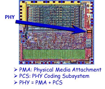
Last point: the Multi-standard SerDes (pictured above) has been successfully deployed in 20+ customer projects and the IP solution integrates MAC/PCS/PMA, another guarantee of faster TTM.

To learn more about IP port-folio from GUC, just go here.

By Eric Esteve from IPNEST


Startups: the Biggest Challenge

Startups: the Biggest Challenge
by Paul McLellan on 01-31-2013 at 9:00 pm

What is the biggest challenge facing an EDA startup today? By a startup, I mean a brand new company, not a company that already has a few customers and is either on a fast path to success or a slower path whereby the company can continue to grow slowly forever.

Obviously, one challenge is the funding environment. Since EDA acquisitions have typically been at low valuations, this has put investors off starting EDA companies. Of course there have been exceptions: Apache and Denali were acquired for healthy valuations but it took a long time to get there in both cases. But with computers so cheap, cloud computing providing almost infinite resource when you need it, and modern programming tools, the amount of money required to get “ramen profitable” is a lot less than it used to be. Another challenge for EDA funding is that it doesn’t need enough money to interest VCs, who have large funds and want to invest the fund in a manageable number (board meetings etc) of large investments.

But I think money is easier to get hold of than something else critical: test-cases.

To be successful as a startup, you have to intercept the future, create technology that isn’t essential today (or someone would already have created it) but will be when you are ready, maybe at 14nm or 10nm. If you are targeting 20nm or above it’s already too late. There are only a handful of groups doing anything at all at 14nm, so how do you get them to work with you?

Answer: you can’t, at least initially. So you have to create your own test-cases to get the product developed. The trouble is that it isn’t clear what the characteristics of a good test-case are. Say someone gives you a 45nm design (even that might be a big ‘if’). How do you need to change it to be a good archetype for a 10nm design. Must be larger for sure. All those sub-20nm stuff like double patterning and layout-dependent-effects. Plus some stuff that probably nobody knows yet.

This was brought home to me during the time I was CEO of Envis. We had some power reduction technology that worked really well on the test-cases we had, reducing power (and occasionally area) by 30% or so. But those designs were old designs that had been designed during an era when power wasn’t an issue so there was lots of low-hanging fruit to be harvested. When we engaged with real customers on real designs, the power savings dropped to more like 7-8%. Not nothing, but not compelling enough for anyone to upend their design methodology.

Another challenge in EDA today is that I think many of the problems are becoming too big for a startup to handle. TSVs require changes to the entire tool flow of the big guys, not just adding a new point tool into the mix. Double patterning, ditto. FinFETs, not a point tool. I’m sure there are niches but that is a problem. Niches are small. To be successful as an EDA startup you need to have something that everyone is going to require eventually, and preferably need lots of licenses. The big guys will eventually have one but maybe you can be first. And best. And if you are, one of the big guys will probably get theirs by buying you.

But you have to get to the point of having something compelling enough to get leading edge groups to engage with you before you get your hands on a real leading edge test-case. Chickens and eggs come to mind.