ASIC design service companies are an essential piece of the SC ecosystem, as well as Silicon Foundries, EDA and IP vendors. Their customers range from pure fabless with no ASIC design resources, who need a third party to turn a concept into a real product (IC) and then market and sale it, to large IDM temporarily lacking design resource to support a project. For a small fabless, building an efficient ASIC design team require a strong investment, covering H/W, up-to-date and expansive EDA licenses and also key peoples, able to successfully manage a project as well as a design team. All of the above represents a lot of energy that the management would have to spend, when the most important part of their job is the market understanding leading to the definition of the ideal system or of the “killer application” which will make their company successful. Using a third party can also be the best way to avoid traps linked to advanced ASIC technology and secure the go-to-market strategy.

Selecting an ASIC design service tightly coupled with a Silicon Foundry, like GlobalUniChip (GUC) is with TSMC is another step to a successful product release, especially during the ramp-up to production. In fact, even if your prototype is first time right, if you are not able to quickly ship the IC to your customers to support their production needs, best case you will delay the revenue flow… worst case a competitor will win the race just on the line! If you’re a Qualcomm or an Apple, you probably build a joint team with TSMC, when the size of the company is more modest, it can be useful to benefit from a well-trained team of Product Engineers, able to manage the Test, Packaging and knowing the target process. Such a service should be offered by an ASIC design service.
This (rather long) introduction help understanding what should be the positioning of ASIC Design Service, in general, and what is effectively the way GUC is running. Designing an ASIC today is often synonym to developing a large SoC. Thus, integrating pre-existing and Silicon proven IP is an absolute requirement. Pre-existing IP to speed-up the design integration, and silicon proven to minimize the risk. The design service company could decide to externally source complexes functions like Interface IP (USB3.0/2.0/1.0, HDMI V1.4 TX and RX for example) or DDR2/3 Memory Controller and PHY, to name a very few, but integrating internally developed IP will be much faster: it will ease the vendor/customer relationship, avoiding to insert another third party, and even more important, the design team will quicker integrate an already known function. Both will positively impact the design cycle, and finally improve the Time-to-Market (TTM).

GUC’s IPs are silicon and production proven in the ASIC projects of a global customer base, and provides designers with a broad range of synthesizable implementation IP, hardened PHYs and verification IP for ASIC, FPGA, and SoC designs. The GUC in-house IP portfolio includes bus interface, mixed signal, data converter, multimedia, power management, and SERDES.
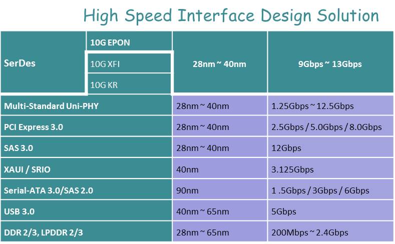
- Bus Interface IP includes digital and mixed-signal standards-based connectivity IP such as 1G and 10G SerDes (supporting GPON/EPON applications as well as XFI and 10G BASE-KR back plane applications), PCI-e 3.0/2.0, SATA 3.0/2.0/1.0, SAS 2/1, USB3.0/2.0/1.0, HDMI V1.4 TX and RX, Interlaken/Double XAUI, XAUI, SGMII, SRIO, Fiber Channel, AHB/AXI, and Ethernet.
- Data Converter IP includes SAR and pipelined ADCs and wide bandwidth, precision and high speed DACs.
- Mixed-Signal IP includes LVDS, power management, DC-DC converters, clock generator IP, 3.3V/2.5V high voltage tolerant/drive I/O, etc.
- Memory Element IP includes many offerings from TSMC including single- and dual-port memory compilers and memory types are also available.
- Peripheral Core IP includes DDR2/3 Controller and PHY IP up to 1600Mbps silicon-proven IP (next generation targeting 2133Mbps) with both wire bond and flip chip solutions.
- Processor IP includes MCU/MPU and hardened ARM processor cores including an ARM development platform for quick prototyping.
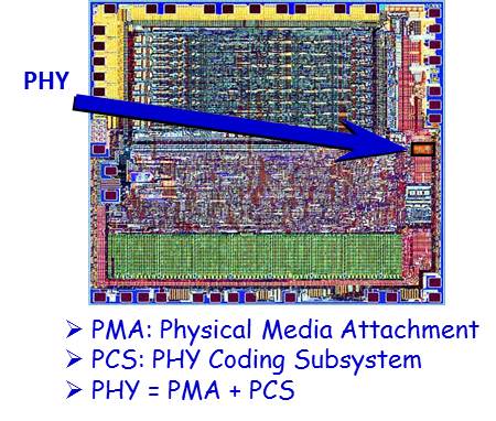
Last point: the Multi-standard SerDes (pictured above) has been successfully deployed in 20+ customer projects and the IP solution integrates MAC/PCS/PMA, another guarantee of faster TTM.
To learn more about IP port-folio from GUC, just go here.
By Eric Esteve from IPNEST


Solving the EDA tool fragmentation crisis